UI Processor Board
- Debug Header
- Data Header
- Power Header
- UART1 Header
- LCD-connector
- USB-connector
- SDRAM Memory
- Flash Memory
- EEPROM
- Buzzer
- LEDs
- BOOT0 Header
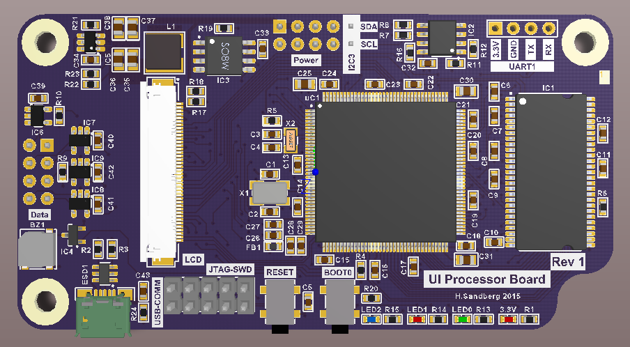
Top View
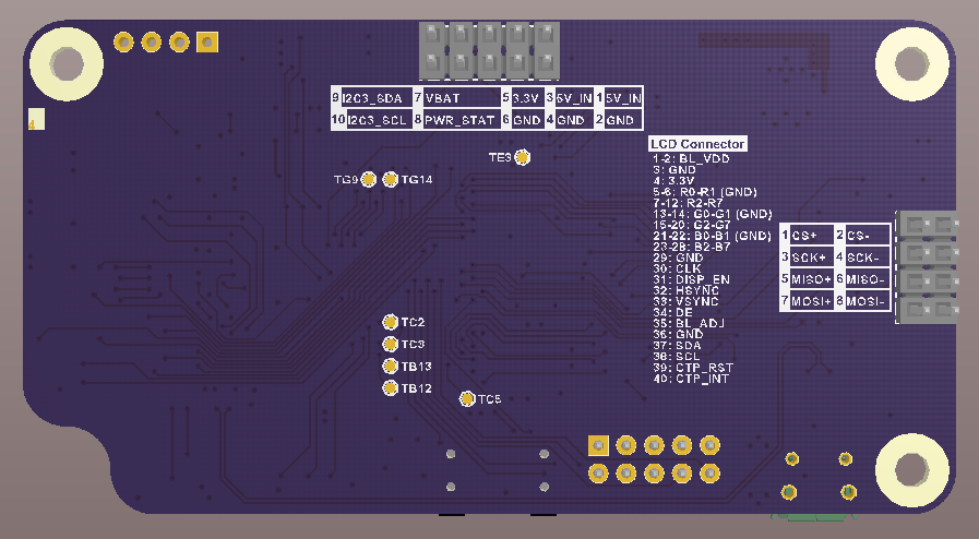
Bottom View
Schematics can be found here.
The MCU is a STM32F429ZI which is basically an ARM Cortex-M4 with some convenient graphics peripherals. Some key features are:
- SDRAM interface
- Chrom-ART Accelerator (DMA2D) for handling graphics
- LCD controller
- A lot of communication interfaces (SPI, I2C, etc)
- 2MB of flash memory
- Real time clock (RTC)
The JTAG-SWD connector has the following pinout:
| Header | Name | MCU |
|---|---|---|
| 1 | 3.3V | - |
| 2 | JTMS-SWDIO | PA13 |
| 3 | GND | - |
| 4 | JTCK-SWCLK | PA14 |
| 5 | GND | - |
| 6 | JTDO | PB3 |
| 7 | (KEY) | - |
| 8 | JTDI | PA15 |
| 9 | GND | - |
| 10 | NJTRST | PB4 |
The data header is used to communicate with the data processor board. To avoid problems with ground loops and other nasty things the SPI signals coming from the MCU is converted to LVDS signals that are available at the header. It has the following pinout:
| Header | Name | MCU After LVDS Driver/Receiver |
|---|---|---|
| 1 | SPI5_nCS_P | PF6 |
| 2 | SPI5_nCS_N | PF6 |
| 3 | SPI5_SCK_P | PF7 |
| 4 | SPI5_SCK_N | PF7 |
| 5 | SPI5_MISO_N | PF8 |
| 6 | SPI5_MISO_P | PF8 |
| 7 | SPI5_MOSI_P | PF9 |
| 8 | SPI5_MOSI_N | PF9 |
The power header provides the power to the board in from a 5V supply. It also has a pin with 3.3V coming from the board so that it can power external devices with 3.3V. VBAT is used to power the RTC when no external power is present on the 5V_IN pin, this makes sure the clock is still running. A POWER_STAT pin is used in conjunction with the connector board to tell which power source is in use. The I2C interface can be used for external communication with for example a "smart" battery pack.
| Header | Name | MCU |
|---|---|---|
| 1 | 5V_IN | - |
| 2 | GND | - |
| 3 | 5V_IN | - |
| 4 | GND | - |
| 5 | 3.3V | - |
| 6 | GND | - |
| 7 | VBAT | - |
| 8 | POWER_STAT | PB7 |
| 9 | I2C3_SDA | PC9 |
| 10 | I2C3_SCL | PA8 |
UART1 is available here to be used for debugging, bootloading or to connect some external peripheral. The pinout is:
| Header | Name | MCU |
|---|---|---|
| 1 | 3.3V | - |
| 2 | GND | - |
| 2 | UART1_TX | PA9 |
| 3 | UART1_RX | PA10 |
The LCD connects to the board using a 40-pin 0.5mm pitch flat flex cable (FPC/FFC) which can be found easily on eBay or any other place. The pinout is:
| FFC | Name | MCU |
|---|---|---|
| 1 | BL_VDD* | - |
| 2 | BL_VDD* | - |
| 3 | GND | - |
| 4 | 3.3V | - |
| 5 | LCD_R0** | - |
| 6 | LCD_R1** | - |
| 7 | LCD_R2 | PC10 |
| 8 | LCD_R3 | PB0 |
| 9 | LCD_R4 | PA11 |
| 10 | LCD_R5 | PA12 |
| 11 | LCD_R6 | PB1 |
| 12 | LCD_R7 | PG6 |
| 13 | LCD_G0** | - |
| 14 | LCD_G1** | - |
| 15 | LCD_G2 | PA6 |
| 16 | LCD_G3 | PG10 |
| 17 | LCD_G4 | PB10 |
| 18 | LCD_G5 | PB11 |
| 19 | LCD_G6 | PC7 |
| 20 | LCD_G7 | PD3 |
| 21 | LCD_B0** | - |
| 22 | LCD_B1** | - |
| 23 | LCD_B2 | PD6 |
| 24 | LCD_B3 | PG11 |
| 25 | LCD_B4 | PG12 |
| 26 | LCD_B5 | PA3 |
| 27 | LCD_B6 | PB8 |
| 28 | LCD_B7 | PB9 |
| 29 | GND | - |
| 30 | LCD_CLK | PG7 |
| 31 | LCD_DISP_ENABLE | PC4 |
| 32 | LCD_HSYNC | PC6 |
| 33 | LCD_VSYNC | PA4 |
| 34 | LCD_DE | PF10 |
| 35 | LCD_BL_ADJ*** | PA7 |
| 36 | GND | - |
| 37 | I2C3_SDA | PC9 |
| 38 | I2C3_SCL | PA8 |
| 39 | CTP_RST | PA2 |
| 40 | CTP_INT | PA1 |
* Backlight power supply, can be set to 5V or 3.3V using jumper R18 and R17
** Grounded pins
*** TIM3_CH2 can be used for PWM on LCD_BL_ADJ
Please note that a 40-pin LCD can NOT be plugged into this connector directly as the board does not have a LED driver on it. To avoid any damage to anyone doing this anyway, pin 1 and 2 of the connector is connected to the same voltage BL_VDD which means that no current will flow trough the LCDs backlight which has VLED- on pin 1 and VLED+ on pin 2. The last four pin are also different from most 40-pin LCD which use these for any resistive touch panel that might be present.
TODO: Adapter board with LED driver so that one can connect a 40-pin LCD easily without using the big LCD board?
| Name | MCU |
|---|---|
| HS_USB_N | PB14 |
| HS_USB_P | PB15 |
A 64-Mbit SDRAM is used as a buffer for the LCD and as a buffer for the graphics. More information on how this is handled can be found on the Simple GUI page.
TODO: Leave some memory for the user to store other things from the external flash for example.
| SDRAM | Signal Name | MCU |
|---|---|---|
| SDRAM_nCS | SDNE1 | PB6 |
| SDRAM_nWE | SDNWE | PC0 |
| SDRAM_nRAS | SDNRAS | PF11 |
| SDRAM_nCAS | SDNCAS | PG15 |
| SDRAM_CLK | SDCLK | PG8 |
| SDRAM_CKE | SDCKE1 | PB5 |
| SDRAM_DQM0 | NBL0 | PE0 |
| SDRAM_DQM1 | NBL1 | PE1 |
| SDRAM_BA0 | BA0 | PG4 |
| SDRAM_BA1 | BA1 | PG5 |
| SDRAM_A0 | RAM_A0 | PF0 |
| SDRAM_A1 | RAM_A1 | PF1 |
| SDRAM_A2 | RAM_A2 | PF2 |
| SDRAM_A3 | RAM_A3 | PF3 |
| SDRAM_A4 | RAM_A4 | PF4 |
| SDRAM_A5 | RAM_A5 | PF5 |
| SDRAM_A6 | RAM_A6 | PF12 |
| SDRAM_A7 | RAM_A7 | PF13 |
| SDRAM_A8 | RAM_A8 | PF14 |
| SDRAM_A9 | RAM_A9 | PF15 |
| SDRAM_A10 | RAM_A10 | PG0 |
| SDRAM_A11 | RAM_A11 | PG1 |
| SDRAM_A12 | RAM_A12 | PG2 |
| SDRAM_D0 | RAM_D0 | PD14 |
| SDRAM_D1 | RAM_D1 | PD15 |
| SDRAM_D2 | RAM_D2 | PD0 |
| SDRAM_D3 | RAM_D3 | PD1 |
| SDRAM_D4 | RAM_D4 | PE7 |
| SDRAM_D5 | RAM_D5 | PE8 |
| SDRAM_D6 | RAM_D6 | PE9 |
| SDRAM_D7 | RAM_D7 | PE10 |
| SDRAM_D8 | RAM_D8 | PE11 |
| SDRAM_D9 | RAM_D9 | PE12 |
| SDRAM_D10 | RAM_D10 | PE13 |
| SDRAM_D11 | RAM_D11 | PE14 |
| SDRAM_D12 | RAM_D12 | PE15 |
| SDRAM_D13 | RAM_D13 | PD8 |
| SDRAM_D14 | RAM_D14 | PD9 |
| SDRAM_D15 | RAM_D15 | PD10 |
The board has a 16-Mbit flash memory that can be used to store large images that are to be used on the display for example.
| Name | MCU |
|---|---|
| SPI4_SCK | PE2 |
| FLASH_nCS | PE4* |
| SPI4_MISO | PE5 |
| SPI4_MOSI | PE6 |
* Has pull-up resistor to 3.3V
A 256Kbit EEPROM is available on the board for storing data. This can be used to save settings or other things that need to be retained after the power to the board has been removed.
| Name | MCU |
|---|---|
| EEPROM_WP | PC8* |
| I2C3_SDA | PC9 |
| I2C3_SCL | PA8 |
| Name | MCU | Timer |
|---|---|---|
| BUZZER | PA0 | TIM5_CH1 |
| Name | MCU |
|---|---|
| LED_0 | PD11 |
| LED_1 | PD12 |
| LED_2 | PD13 |
| Header | Name |
|---|---|
| 1 | 3.3V |
| 2 | BOOT0 |
The board is 4 layer, 85x45 mm. It has three mounting holes that can be used to secure it to a case or another board.
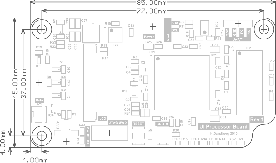
Mechanical Drawing