FPGA ID Reader
To be able to distinguish between what type of module is installed for each channel an ID is assigned to each module, more info about this can be found on the Module IDs page. This is basically an analog voltage that is converted to a digital value in the FPGA by using an external analog to digital converter (ADC).
On the DE0-Nano development board I'm using for the prototyping there is a ADC128S022 chip on board and for the final version I will use something similar. The digital interface will be SPI as explained below.
TODO
More detailed information about the interface can be found on Wikipedia and in the datasheet for the ADC.
The master SPI controller I've made can be configured for different data widths and has a prescaler to scale down the input clk to a valid sclk for the SPI device we are trying to control.
Interfacing with the SPI module is quite straightforward and kept as simple as possible. Before starting a transfer the user of the module has to check the busy_transfer signal to make sure the module is not currently doing a transfer. If that signal is low a transfer can be started by setting data_to_send to the data which you want to send and then asserting the start_transfer. The next clk cycle the SPI module will store the value of data_to_send internally and it will assert the busy_transfer to notify the user that it has started processing. After all bits have been transferred busy_transfer will be pulled low and at the same time valid_data goes high to indicate that data has been read from the SPI slave and is now available for the user to read on data_received.
A simulation of two 16-bit transfers can be seen below:
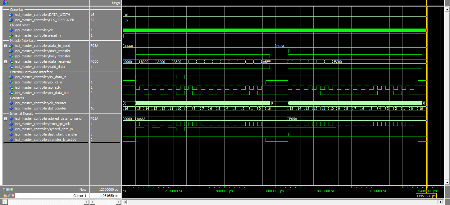
Two 16-bit SPI transfers
Now that we have a working SPI master controller we need to use to send the appropriate data to use the ADC.
For the ADC128S022 we have to send 16 bits each time as described in the datasheet on page 7. The third, fourth and fifth bit we send sets the channel which will be sampled the next time, i.e. we send a command for a channel N and then the next time we send a command we can read the data for channel N. This can be seen in the simulation below by looking at the tb_spi_data_out signal which is basically counting from 0 to 7 and then repeating this.
To get a more stable value the ADC controller is using averaging. The number of averages is set by a generic to a certain power of two, i.e. if the generic NUM_OF_AVERAGES_AS_POWER_OF_TWO is set to 4 it means 2^4 = 16 averages will be used. The averaging used is not a moving average but instead it adds N number of samples and then divides this sum by N and outputs it to the chX_value signals. When the outputs are updated the valid_values signal goes high as well to indicate to the user new data is available.
A simulation of the ADC testbench can be seen below. In this simulation the averaging is set to 2^1 = 2 which can be seen by counting the number of valid_data pulses between two valid_values pulses. Here it is 16 which is two times the number of channels.
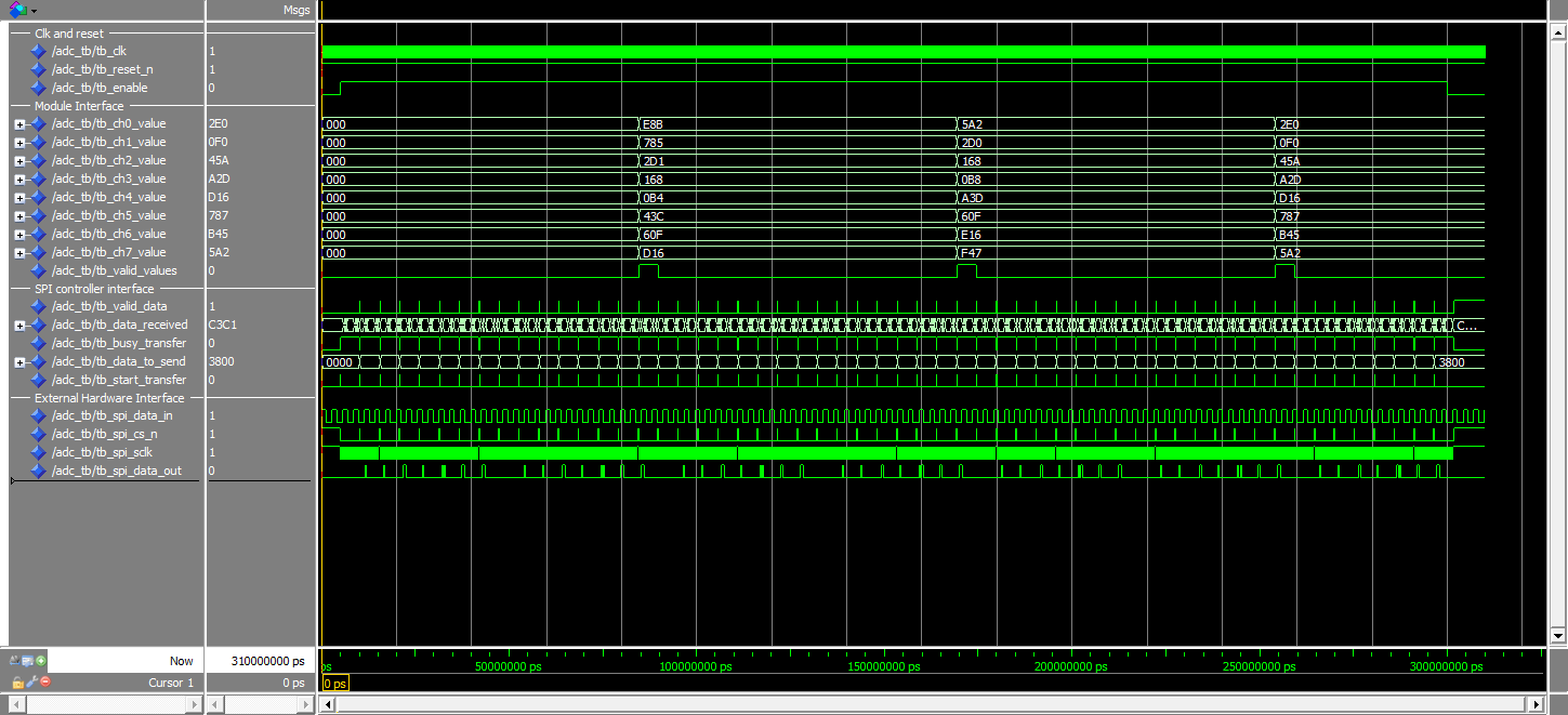
ADC Testbench
TODO Better to update each channel separately???