Data Processor Board
- Data Header
- Power Header
- FPGA
- Clock
- LEDs
- DIP Switch
- SDRAM Memory
- A/D Converter
- I2C Bus
- I/O Connectors
- Debug Header
- Testpads
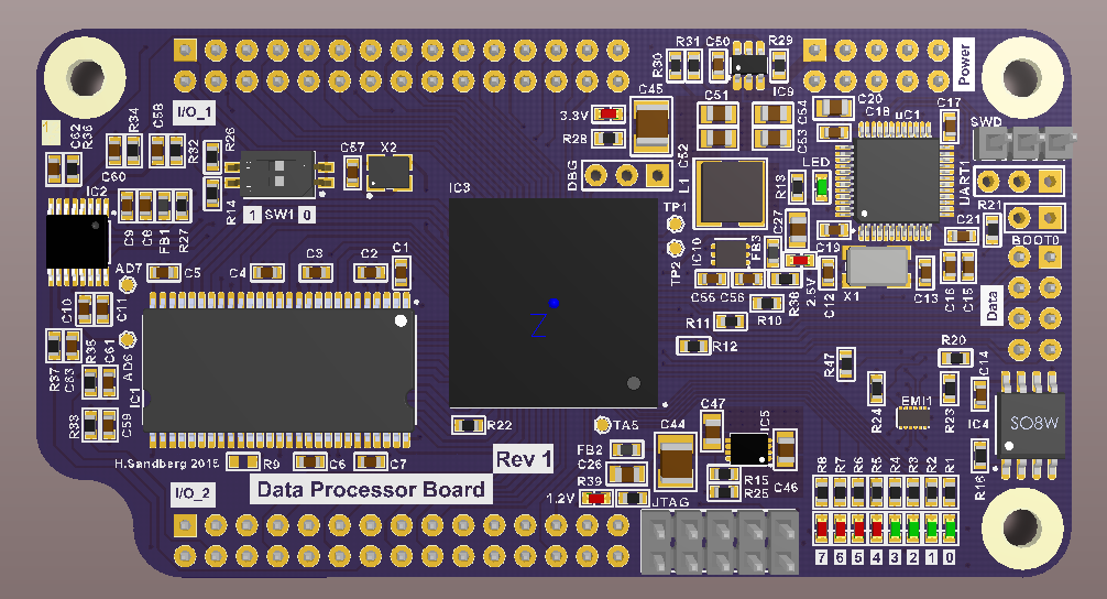
Top View
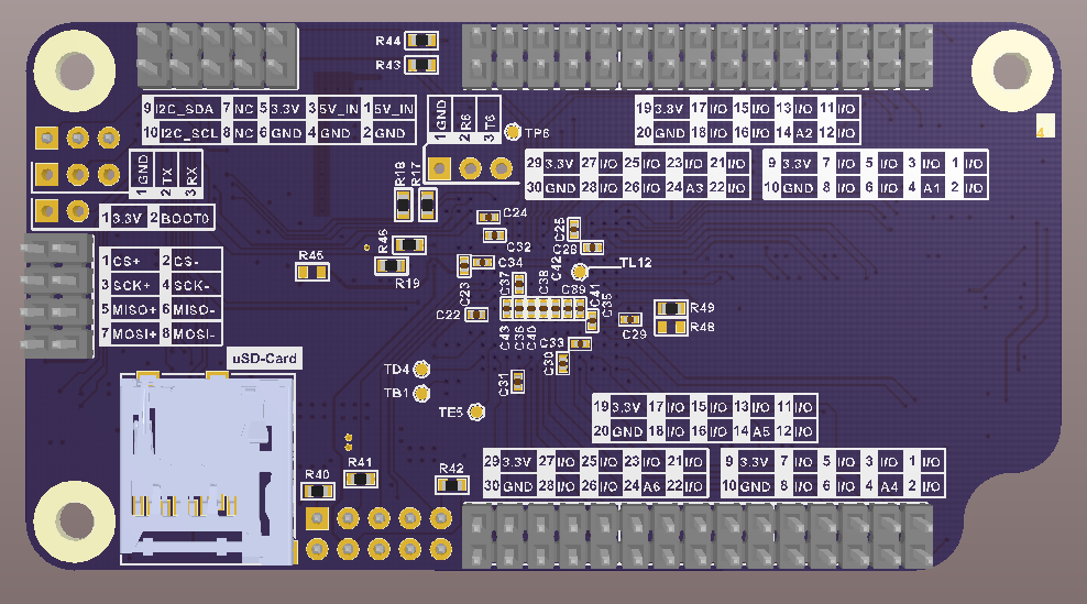
Bottom View
Schematics can be found here.
The BOM can be found here.
The data header is used to communicate with the UI processor board. To avoid problems with ground loops and other nasty things the SPI signals coming from the UI processor is converted to LVDS signals that are available at the header. It has the following connections:
| Header | Name | FPGA |
|---|---|---|
| 1 | SPI_UI_nCS_P | K2 |
| 2 | SPI_UI_nCS_N | K1 |
| 3 | SPI_UI_SCK_P | J2 |
| 4 | SPI_UI_SCK_N | J1 |
| 5 | SPI_UI_MISO_P | G2 |
| 6 | SPI_UI_MISO_N | G1 |
| 7 | SPI_UI_MOSI_P | F2 |
| 8 | SPI_UI_MOSI_N | F1 |
The power header provides the power to the board in from a 5V supply. It also has a pin with 3.3V coming from the board so that it can power external devices with 3.3V.
| Header | Name | FPGA |
|---|---|---|
| 1 | 5V_IN | - |
| 2 | GND | - |
| 3 | 5V_IN | - |
| 4 | GND | - |
| 5 | 3.3V | - |
| 6 | GND | - |
| 7 | NC | - |
| 8 | NC | - |
| 9 | I2C_SDA | N6 |
| 10 | I2C_SCL | L10 |
The FPGA on the board is from Altera's Cyclone IV E family and I chose this because I have a DE0-Nano development board that uses an FPGA from that family as well. As this is my first FPGA design I wanted to make sure it works on a development board first before I moved it over to my custom board. Originally I hade plan on using the EP4CE6E22C8N which is in a 144-EQFP package that is easy to solder but after counting all the I/Os I needed it became obvious this wouldn't work. Therefore I moved to the EP4CE6F17C8N that is in a 256-FBGA package. This means there is enough I/Os but because it's an BGA it's not as easy to solder and will require an oven, but it's manageable.
The EP4CE6F17C8N is the smallest FPGA in the Cyclone IV E family with 6272 logic elements (LEs) and therefore also the cheapest. Hopefully this will be enough but it is always possible to upgrade to EP4CE10F17C8N (10320 LEs) as they are pin-compatible. EP4CE15F17C8N (15408 LEs) and EP4CE22F17C8N (22430 LEs) are not pin-compatible. It is also possible to upgrade to an FPGA with a higher speed grade as these (C8) are not the fastest available, but again the cost will increase.
On the board is a 50MHz MEMS oscillator as standard, part number 501AAA50M0000CAF. It is connected to two of the clock pins on the FPGA.
Connections:
| Clock | FPGA |
|---|---|
| CLK_50M | M15 |
| CLK_50M | M16 |
There are in total eight LEDs on the board connected to the FPGA. A logic HIGH will turn the LED on and a logic LOW will turn it off.
Connections:
| LED | FPGA |
|---|---|
| LED_0 | D3 |
| LED_1 | C3 |
| LED_2 | A2 |
| LED_3 | B3 |
| LED_4 | A3 |
| LED_5 | B4 |
| LED_6 | A4 |
| LED_7 | B5 |
Connections:
| DIP Switch | FPGA |
|---|---|
| DIP_SW0 | M7 |
| DIP_SW1 | M8 |
To store data there is a 64-Mbit SDRAM on the board, the same type that is used for the UI Processor Board (to save cost). The data bus is 16-bit wide (D0-D15) and the address bus is 13bits (A0-A12) to support bigger SDRAMs.
Connections:
| SDRAM | FPGA |
|---|---|
| SDRAM_nCS | N13 |
| SDRAM_nWE | L13 |
| SDRAM_nRAS | L16 |
| SDRAM_nCAS | L15 |
| SDRAM_CLK | B14 |
| SDRAM_CKE | C15 |
| SDRAM_DQM0 | L14 |
| SDRAM_DQM1 | C14 |
| SDRAM_BA0 | N14 |
| SDRAM_BA1 | N15 |
| SDRAM_A0 | P16 |
| SDRAM_A1 | R16 |
| SDRAM_A2 | G16 |
| SDRAM_A3 | G15 |
| SDRAM_A4 | F16* |
| SDRAM_A5 | F15 |
| SDRAM_A6 | F14 |
| SDRAM_A7 | F13 |
| SDRAM_A8 | D16 |
| SDRAM_A9 | D15 |
| SDRAM_A10 | N16 |
| SDRAM_A11 | C16 |
| SDRAM_A12 | D14 |
| SDRAM_D0 | J13 |
| SDRAM_D1 | J14 |
| SDRAM_D2 | J12 |
| SDRAM_D3 | J15 |
| SDRAM_D4 | J16 |
| SDRAM_D5 | K12 |
| SDRAM_D6 | K15 |
| SDRAM_D7 | K16 |
| SDRAM_D8 | B16 |
| SDRAM_D9 | A15 |
| SDRAM_D10 | A14 |
| SDRAM_D11 | D12 |
| SDRAM_D12 | A13 |
| SDRAM_D13 | B13 |
| SDRAM_D14 | A12 |
| SDRAM_D15 | B12 |
* In Quartus: Go to Assignments > Device > Device and Pin Options > Dual-Purpose Pins nCEO -> use as regular IO
Each I/O module has an ID pin that is just an analog voltage that the data processor has to read, more information can be found on the module ids page. This is done using a ADC108S022, 8 channel, 10-bit, 50-200ksps A/D converter. As speed is not important and the required resolution is actually 5-bits (32 different IDs) this A/D converter is good enough.
Connections:
| ADC | FPGA |
|---|---|
| SPI_AD_SCLK | N12 |
| SPI_AD_MOSI | P14 |
| SPI_AD_MISO | P15 |
| SPI_AD_nCS | R14 |
Connections:
| I2C | FPGA |
|---|---|
| I2C_SDA | N6 |
| I2C_SCL | L10 |
Connections:
| Header Pin | Name | Module | FPGA |
|---|---|---|---|
| I/O_1-1 | I/O_1AB_P | 1-IN_A | T14 |
| I/O_1-2 | I/O_1AB_N | 1-IN_B | T15 |
| I/O_1-3 | I/O_1C | 1-IN_C | M10 |
| I/O_1-4 | ID_1 | 1-IN_D | - |
| I/O_1-5 | I/O_1EF_P | 1-IN_E | R13 |
| I/O_1-6 | I/O_1EF_N | 1-IN_F | T13 |
| I/O_1-7 | I/O_1GH_P | 1-IN_G | R12 |
| I/O_1-8 | I/O_1GH_N | 1-IN_H | T12 |
| I/O_1-9 | 3.3V | 1-IN_VLOGIC | - |
| I/O_1-10 | GND | - | - |
| I/O_1-11 | I/O_2AB_P | 2-IN_A | R11 |
| I/O_1-12 | I/O_2AB_N | 2-IN_B | T11 |
| I/O_1-13 | I/O_2C | 2-IN_C | M9 |
| I/O_1-14 | ID_2 | 2-IN_D | - |
| I/O_1-15 | I/O_2EF_P | 2-IN_E | R10 |
| I/O_1-16 | I/O_2EF_N | 2-IN_F | T10 |
| I/O_1-17 | I/O_2GH_P | 2-IN_G | R9 |
| I/O_1-18 | I/O_2GH_N | 2-IN_H | T9 |
| I/O_1-19 | 3.3V | 2-IN_VLOGIC | - |
| I/O_1-20 | GND | - | - |
| I/O_1-21 | I/O_3AB_P | 3-IN_A | R8 |
| I/O_1-22 | I/O_3AB_N | 3-IN_B | T8 |
| I/O_1-23 | I/O_3C | 3-IN_C | N9 |
| I/O_1-24 | ID_3 | 3-IN_D | - |
| I/O_1-25 | I/O_3EF_P | 3-IN_E | N8 |
| I/O_1-26 | I/O_3EF_N | 3-IN_F | P8 |
| I/O_1-27 | I/O_3GH_P | 3-IN_G | R7 |
| I/O_1-28 | I/O_3GH_N | 3-IN_H | T7 |
| I/O_1-29 | 3.3V | 3-IN_VLOGIC | - |
| I/O_1-30 | GND | - | - |
- | - | - | - I/O_2-1 | I/O_4AB_P | 4-IN_A | D11 I/O_2-2 | I/O_4AB_N | 4-IN_B | C11 I/O_2-3 | I/O_4C | 4-IN_C | F11 I/O_2-4 | ID_4 | 4-IN_D | - I/O_2-5 | I/O_4EF_P | 4-IN_E | E9 I/O_2-6 | I/O_4EF_N | 4-IN_F | F10 I/O_2-7 | I/O_4GH_P | 4-IN_G | B11 I/O_2-8 | I/O_4GH_N | 4-IN_H | A11 I/O_2-9 | 3.3V | 4-IN_VLOGIC | - I/O_2-10 | GND | - | - I/O_2-11 | I/O_5AB_P | 5-IN_A | B10 I/O_2-12 | I/O_5AB_N | 5-IN_B | A10 I/O_2-13 | I/O_5C | 5-IN_C | C9 I/O_2-14 | ID_5 | 5-IN_D | - I/O_2-15 | I/O_5EF_P | 5-IN_E | B9 I/O_2-16 | I/O_5EF_N | 5-IN_F | A9 I/O_2-17 | I/O_5GH_P | 5-IN_G | B8 I/O_2-18 | I/O_5GH_N | 5-IN_H | A8 I/O_2-19 | 3.3V | 5-IN_VLOGIC | - I/O_2-20 | GND | - | - I/O_2-21 | I/O_6AB_P | 6-IN_A | D9 I/O_2-22 | I/O_6AB_N | 6-IN_B | C8 I/O_2-23 | I/O_6C | 6-IN_C | D8 I/O_2-24 | ID_6 | 6-IN_D | - I/O_2-25 | I/O_6EF_P | 6-IN_E | B6 I/O_2-26 | I/O_6EF_N | 6-IN_F | A6 I/O_2-27 | I/O_6GH_P | 6-IN_G | D6 I/O_2-28 | I/O_6GH_N | 6-IN_H | D5 I/O_2-29 | 3.3V | 6-IN_VLOGIC | - I/O_2-30 | GND | - | -
A three pin 2.54mm pitch header is located near the FPGA marked "DBG". This can be used as a serial port for debug information for example.
| Header | Name | FPGA |
|---|---|---|
| 1 | GND | - |
| 2 | DEBUG_0 | R6 |
| 3 | DEBUG_1 | T6 |
Some extra pins on the FPGA are routed to testpads on the top and bottom of the PCB. These are:
| Testpad | FPGA |
|---|---|
| TA5 | A5 |
| TB1 | B1* |
| TD4 | D4* |
| TE5 | E5* |
| TL12 | L12 |
| TP1 | P1** |
| TP2 | P2** |
| TP6 | P6 |
* Connected to bank 2 and therefore VCCIO is 2.5V.
** Connected to bank 2 and can be used as a differential pair. P2 is positive, P1 is negative.
The "problem" with FPGAs is that they have to be configured before they do anything useful. Basically when power is first applied and the FPGA goes out of reset it just sits there doing nothing as the HDL-design we want to run on the FPGA is lost when power is removed (simple RAM storage). We therefore have to send all the data for our design to the FPGA so that is can be configured. There are many different ways this can be done and more information about it can be found in chapter 8 of the Cyclone IV Handbook (Caution: Big PDF!!!). I've chosen to use "PS Configuration Using an External Host" (chapter 8-33) which basically means that an MCU sends all the data to the FPGA using a SPI-ish interface.
For this a STM32F103C8T6 is used, mainly because it can be bought dirt-cheap from China. It has two SPI interfaces that are used to interface with the FPGA, Flash memory and SD-card.
- SPI1: FLASH and FPGA data
- SPI2: SD Card and FPGA config
On power-up the MCU will check in the external Flash memory for a valid bit file which it then configures the FPGA with. TODO: List of all the steps needed during configuration to check for errors and such
A second task for the MCU is to handle the communication with the MicroSD Card. Originally it was planned to implement a soft processor inside the FPGA that would interface to the SD-card but it became obvious it would take more time and also create a problem if a Xilinx FPGA would be used in a future data processor board. By having the MCU control the SD-card it is also possible to use it for FPGA configuration updates. By loading a bit file on the card the MCU can read that and store it in the external Flash and later configure the FPGA with this new bit file.
Connections between FPGA and config MCU:
| Config MCU | Function | FPGA |
|---|---|---|
| PA5 | SPI1_SCK | P3 |
| PA6 | SPI1_MISO | T3 |
| PA7 | SPI1_MOSI | R3 |
| PB0 | FPGA_nCS* | T2 |
| PB1 | FPGA_INTERRUPT* | T5 |
| PA8 | nCONFIG* | H5 |
| PB11 | nSTATUS* | F4 |
| PB10 | CONF_DONE* | H14 |
| PB13 | SPI2_SCK | H1 |
| PB15 | SPI2_MOSI | H2 |
* Has pull-up resistor to 3.3V
The external SPI Flash is a 16-Mbit, same as on the UI Processor Board. It is used to store the configuration file for the FPGA. A configuration file for the EP4CE6F17C8N is 2944088 bits which means we can store 16777216/2944088 = 5,69 -> 5 configuration files in the flash.
TODO Image of memory organization
| uSD-Card Pin | Name | Config MCU |
|---|---|---|
| 1 | - | - |
| 2 | SD_CARD_nCS* | PB12 |
| 3 | SPI2_MOSI | PB15 |
| 4 | 3.3V | - |
| 5 | SPI2_SCK | PB13 |
| 6 | GND | - |
| 7 | SPI2_MISO | PB14 |
| 8 | - | - |
| 9 | GND** | - |
| 10 | CARD_DETECT* | PA3 |
* Has pull-up resistor to 3.3V
** One contact of the card-detect switch
UART1 is available here to be used for debugging, bootloading or to connect some external peripheral. The pinout is:
| Header | Name | Config MCU |
|---|---|---|
| 1 | GND | - |
| 2 | UART1_TX | PA9 |
| 3 | UART1_RX | PA10 |
| Header | Name | Config MCU |
|---|---|---|
| 1 | SWCLK | PA14 |
| 2 | GND | - |
| 3 | SWDIO | PA13 |
| Header | Name |
|---|---|
| 1 | 3.3V |
| 2 | BOOT0 |
The board is 4 layer, 85x45 mm. It has three mounting holes that can be used to secure it to a case or another board.
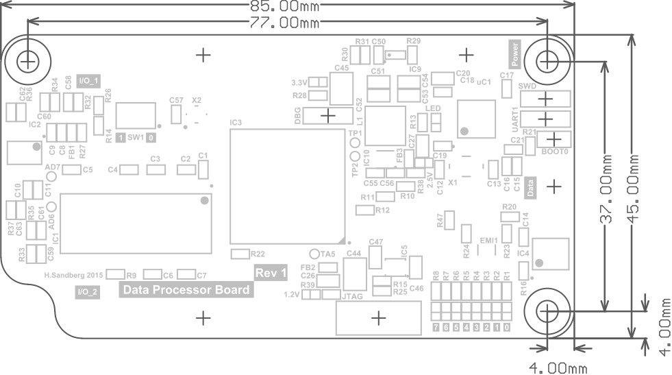
Mechanical Drawing