Board CN2596
Certain very low cost LM2596 based DC/DC converters with an STM8S003F3P6 based voltmeter can be modified into a programmable power supply with little effort. There is an ongoing project Low-Cost Programmable Power Supply on Hackaday.io, which demonstrates use cases like automotive power-supply robustness test ("cold-cranking").
Note: there is a new "DCDC converter with voltmeter" available that's even more hackable than the old one. Check out the STM8 eForth DCDC configuration folder and the Hack-A-Day log - New modding instructions will be published in a while! - You can, of course, join on HaD, or in issue #286.
Release v2.2.8 introduces support for modified CN2596-2 boards.
The following instructions assume the module type in the picture below. When purchasing modules, search for "LM2596 1.3-37V Step-Down", and look for green (rarely blue) PCBs, with a LM317 in a TO92 package (avoid the slightly larger blue ones with the LM317 in a SOT223 SMD package).
In order to control the LM2596 with the voltmeter µC some simple modifications of the board are required. The picture below shows a fully modified board.
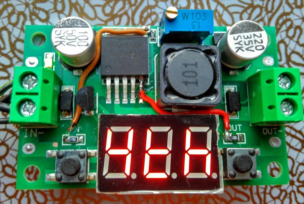
- remove LED "IN"
- remove LED "OUT"
- interrupt the connection between LM2596 pin 5 (!ON/OFF) and GND (i.e. cut the pin in the middle, and de-solder the lower half)
- cut the copper trace between LM317 pin2 and anode pad of LED "IN". Expose some of the copper of the trace near the LED pad.
- carefully cut the copper trace between the LM2596 heat sink (GND), and the 330R between the LM2596 and the trimmer.
- solder a 10µF ceramics capacitor 0603 or 0805 to the (newly cut) copper trace between the LM2596 heat sink GND and the pad of the 330R next to the trimmer (see picture)
- solder a C 100nF between LM317 pin 2 and GND on the backside of the PCB
- solder a 47R 0805 resistor to the pads of LED "IN"
- solder a 1k8 0805 resistor to the pads of LED "OUT"
- add a wire between the copper trace near the anode pad of LED "IN" (PC3) to the 330R pad (where the 10µF capacitor is connected)
- add a wire between the cathode pad of LED "OUT" (PB4) and LM2596 pin 5
- add a 2 pin programming connector to GND and pin 4 of the 7S-LED display (segment C, PD1/SWIM).
- get the binary from the v2.2.8 release (or later)
- programming the STM8S003F3P6 with an ST-LINK adapter by programming SWIM and GND to the programming connector
- solder the anode of a 1N4148 diode to pin 3 of the 7S-LED display (segment DP, PC7).
- wire a 3 pin connector to pin 3 of the display, the cathode of the 1N4148, and to GND.
- start a terminal program (preferably e4thcom) at 9600 baud, and test the connection by pressing ENTER
The following sketch shows the improvised 2-wire communication interface:
CN2596             .----o serial TxD "TTL"
                   |      (e.g. "PL2303" USB serial converter")
                  ---
                  / \  1N4148
                  ---
7S-LED pin3        |
                   |
STM8 PC7/DP  ------*----o serial RxD "TTL

  GND ------------------o serial GND
Note: the serial interface works in "half-duplex" mode without collision detection. This works well for normal normal console interaction (e.g. with e4thcom) during which the DP segment remains unused. Non-interactive applications should send a CR until a LF character is received. More details are described here.
Using a voltmeter and the interactive Forth console, the function U=f(PWM) can be estimated. It turned out that between 0 and 1V the function is less smooth, and an extra grid point is needed.

Also, it wasn't possible to get below 20mV output voltage (after all, a bias to the feedback ground of an LM2596 is a hack). The last grid point is 469/20mV.
: @dif ( a -- n )     \ delta of value pairs
  DUP 2+ 2+ @ SWAP @ - ;
: @inter ( x a -- y ) \ find value pairs, interpolate
  DUP @ 1- >R 2+ DUP BEGIN
    2 PICK OVER @ < NOT WHILE
    NIP DUP 2+ 2+ NEXT
      DROP DUP
    ELSE R> DROP THEN \ eForth LEAVE idiom
  OVER = IF           \ pointers equal: saturation
    2+ @ NIP
  ELSE
    DUP ROT OVER @ - OVER 2+ @dif
    ROT @dif */ SWAP 2+ @ + THEN ;
@dif looks up two values returns the difference (X1-X0 or Y1-Y0 depending on the offset). @inter does a table lookup with interpolation. The input is the value and the address of a table with n value pairs (Xn, Yn) ordered by ascending values of X, and preceded by the number of n (the sequence R> ... BEGIN is equivalent to FOR, and the FOR .. WHILE .. NEXT .. ELSE .. THEN is an eForth idiom for an extended DO .. LEAVE .. LOOP structure). Compiled, this code needs just 177 bytes, and since it doesn't use global variables it's 'thread safe'.
Note: e4thcom users can just run #require @inter to load the interpolation word from the STM8 eForth library
When representing the voltage in units of mV, and the following table with 14 grid points does the linearization:
NVM
CREATE vptab
14 ,
469 20 , , 451 500 , , 434 1010 , , 401 2000 , ,
367 3010 , , 333 3990 , , 297 5010 , , 261 5990 , ,
222 7010 , , 183 7990 , , 141 8990 , , 97 9990 , ,
50 11000 , , 0 12000 , ,
RAM
CREATE adds the (empty) word vptab to the dictionary which, when called, pushes the address of the byte following the word's dictionary entry on the stack. The following sequence of interpreted numbers and , attaches 14 pairs X/Y pairs of data to the word vptab. Of course, such lookup functions can be chained, or used to model most functional dependencies (e.g. as a function of time, state, or input).
The mapping of output voltage to PWM is simple:
NVM
: mV vptab @inter pwm ;
RAM
On the console, typing eg. 7500 mV results in an output voltage of 7.53V, which is quite accurate (for being a hack).
Here are more examples:
- 5000 mV -> 5.02V
- 3700 mV -> 3.73V
- 3300 mV -> 3.35V
- 2800 mV -> 2.83V
Because of the saturation feature of @inter the following works, too:
- 15000 mV -> 12.00V
- -10000 mV -> 0.03V
Especially at in a lower output voltage range some drift is to be expected (results can be improved a bit with closed loop control, although there is no voltage reference source).
Professional (and certifiable) programmable power supplies are expensive, and for acceptance testing they are necessary. However, exploratory testing can greatly improve understanding failure modes, and improve the robustness of a product. The programmable power supply can be used to produce some of the test pulses defined in ISO 7637-2:2011. A log entry at Hackaday.io demonstrates this possibility.
There is a blue, and a green variant of the board. The green variant has pads for an ICP (In Circuit Programming), which is a clear advantage. Also, there is a different blue "DCDC module with Voltmeter" available which is more difficult to modify (removal of the 7S-LED display is necessary). The LM317 of this variant is a SMD component, while it's a through-hole component on the "right" boards. However, after removing the 7S-LED display this blue variant can still be used with the method described below.
The STM8S003F3 has a supply voltage of about 3.1V (LM317 with fixed voltage divider), which also serves as the "reference voltage source" for the voltmeter part. Note that there is no capacitor on the 3.1V side of the power supply. Retrofitting at a 1µF capacitor between pin2 of the LM317 and the GND plane is highly recommended!
The green variant of the module has an ICP connector. Retrofitting a 100nF capacitor there is recommended.
Back of PCB, display top
--------------
  (1) VCC  <-- add 100nF between pad and GND plane!
  (2) SWIM
  (3) NRST
  (4) GND
The resolution is about 54mV/digit, and there is just enough noise for some averaging. This also means that the inputs have a range of about 56V.
: vIn ( -- n )
  2 adc! adc@ 100 184 */ ;

: vOut ( -- n )
  4 adc! adc@ 100 184 */ ;
Pin assignments for blue and green variant (ICP connector of green variant in brackets):
Pin	STM	 Connected to
1	PD4	 seg B
2	PD5	 dig 1
3	PD6	 dig 2
4	NRST     (ICP pin 3)
5	PA1	 seg F
6	PA2	 seg A
7	VSS	 GND (ICP pin 4)
8	Vcap	 Cap
9	VDD	 +3.1V (ICP pin 1)
10	PA3	 dig 3
11	PB5	 -
12	PB4	 led "out"
13	PC3	 led "In"
14	PC4	 Vin (analog)
15	PC5	 seg E / key "in"
16	PC6	 seg D
17	PC7	 seg DP
18      PD1/SWIM seg C (ICP pin 2)
19	PD2      seg G / key "out"
20	PD3	 Vout (analog)
As suggested in a discussion on Hackaday the 7S-LED display can be removed and the pads can be used as µC port breakout. This option is maybe attractive for applications that require cheap, and easily available programmable power supply board, but no LED display. GPIOs with additional features (robust communication, SPI, ADC, timers) are readily available at the LED display pads. Pin 6 (NC) can be used as a ground connection for an attached (stacked) circuit board.
Pin     LED      Connected to
1       E        PC5 / key "in"
2       D        PC6
3       DP       PC7
4       C        PD1
5       G        PD2 / key "out"
(6)     -
7       B        PD4
8       dig3     PA3
9       dig2     PD6
10      F        PA1
11      A        PA2
12      dig1     PD5