An Optimal Microarchitecture for Stencil Computation Acceleration Based on Nonuniform Partitioning of Data Reuse Buffers
- About
- Technologies
- Setup
- Introduction
- Single Time-Step
- Multiple Time-Steps
- Detailed Explanation
- References
This project introduces an architecture that optimizes Stencil Kernel Calculations and is offloaded to FPGAs with the use of High Level Synthesis tools (HLS).
Project is created with:
- C/C++
- Vitis HLS 2021.2
- Run Vitis (or Vivado) HLS adding the source & header files from the corresponding folder.
- The jacobi9d.cpp file should be used as the top function for the implementation of a single time-step.
- The Temporal.cpp file should be used as the top function for the implementation of multiple time-steps.
- Utilize the provided Test-Bench from the corresponding folder.
- In the header file the defined size of the grid can be modified.
- The number of Time-Steps can be modified in the Temporal.cpp file, by adding succesive calls to the jacobi9d funncion and declaring the intermediate variables.
This architecture is based on the work done in [1]. The aim of the design developed is to calculate the Jacobi 9-Point kernel for a given 2D grid of arbitrary size. The architecture proposed, introduces a novel method of non-uniform memory partitioning that achieves the theoretical minimum number of memory banks utilized. Moreover, the buffers used, are tailored to the needs of the specific stencil pattern, exploiting data reuse to accomplish the minimum size for these data reuse buffers. Thus, the design realizes the minimum usage of On-Chip Memory (OCM) and the minimum off-chip data accesses. Moreover, it can be characterized by its pipelined architecture, i.e., for every clock cycle, there is one new input from off-chip memory, and one new result outputted by the out ports.
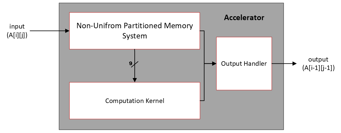
As depicted, there is one input and one output for every clock cycle. The non-uniformly partitioned memory system handles this input and either feeds the 9 data elements required to the computation kernel, or, in the case of halo elements, forwards data directly to the Output Handler. The Computation Kernel’s function is the calculation of the resulting value. The Output Handler ensures the output of the data in lexicographic order and utilizes control logic to select either halo data, or computed results.

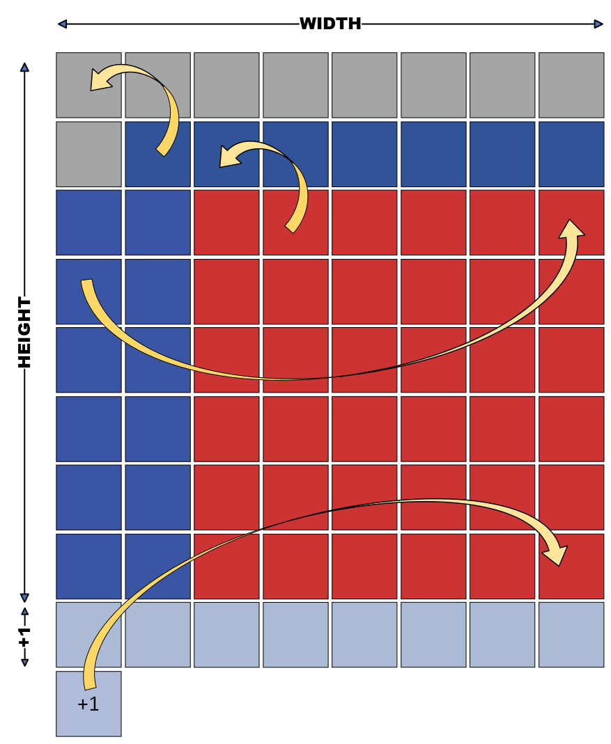
The figure shows a 2D grid, 𝐴[𝐻𝐸𝐼𝐺𝐻𝑇][𝑊𝐼𝐷𝑇𝐻], and the stencil window of a 9-Point Jacobi Kernel sliding over it. To compute the result of one element, 9 elements of the previous time-step need to be available, thus they need to have been stored on-chip and made available for concurrent access. For an arbitrary data element 𝐴𝑡 [𝑖][𝑗], that we compute, it becomes evident that the elements 𝐴𝑡−1[𝑖 − 1][𝑗 − 1] through 𝐴𝑡−1[𝑖 + 1][𝑗 + 1] need to be stored on-chip. The total of these elements is highlighted in highlighted colors (red, blue, and green) in the figure.

The internal structure of the memory system in our design is provided in Figure 11. Since the focus of this thesis is directed at a 𝑛 = 9 points stencil, 𝑛 data reuse registers, that act as independent memory entities, will be utilized to hold the data needed for each computation. Parallel access to those data elements is necessary and justifies the independence among them. Between those registers, the design implements data reuse first-inputs, first-outputs (FIFOs) that provide storage for elements not required for the current computation but still need to be reused in following ones.
On our Xilinx platform, large FIFO, whose capacity is larger than 1024 bits is implemented with BRAM, and small FIFO, is implemented with SRL. In figure 8, the data in the registers are the ones in the red square frame and the data in the FIFOs are the ones in between, highlighted in blue and green. This sequence of registers and FIFOs is addressed as the reuse buffer. As this stencil window slides along the iteration domain, the data in the reuse buffer are propagated in a streaming manner i.e., for each clock cycle, the existing data in the memory units (registers, FIFOs) are passed to the successive unit. As for the input, the module reads one data element from off-chip memory and stores it in register 𝑅_0.

As discussed, the size of the utilized memory units is non-uniform and is in derived from the number of elements stored in them. Depending on their size and functionality they are also mapped to different physical implementations. Considering a 2D array of size 𝐻𝐸𝐼𝐺𝐻𝑇 𝑥 𝑊𝐼𝐷𝑇𝐻 the table bellow provides an overview of the size and physical implementation of each memory unit.
The total size of the reuse buffer will be the sum of the distinct memory units and is also equal to the iteration distance between the first and the last element needed to calculate the result. This is also evident in the optical representation of the figure depicting the grid.
𝑅𝑒𝑢𝑠𝑒_𝐵𝑢𝑓𝑓𝑒𝑟_𝑆𝑖𝑧𝑒 = 2 ∗ 𝑊𝐼𝐷𝑇𝐻 + 3
The Output Handler receives the result of the Calculation Kernel, or the halo element fetched from the reuse buffer. It is noteworthy to mention that the output of an element in an arbitrary grid position [𝑖][𝑗] is only available after the element in [𝑖 + 1][𝑗 + 1] has been read, this is a restraint imposed on the design by the nature of the stencil algorithm. Thus, introducing a delay of 𝑊𝐼𝐷𝑇𝐻 + 1 cycles from the moment that the first input is read, to the moment that the calculation of the first out begins. During this time, the reuse buffer is filled with data that is read from the external memory.
To maintain a continuous data flow on the output port, the halo elements are also delayed 𝑊𝐼𝐷𝑇𝐻 + 1 cycles. Figure 12 provides an overview of how the data are outputted from the module. Disregarding the intrinsic latency of the design, the fist output takes place when the read input iterators arrive at element [1][1], and the data element that is forwarded to the output is the halo element in [0][0], which is fetched to the Output Handler directly from register 𝑅_4. Ergo, when the input iterators traverse the blue data elements, the module outputs halo elements. Contrary when the red elements are read at the input, the output is that of calculated data fetched from the Computation Kernel. The above process maintains the lexicographic order in the outputted results.
It should be taken into consideration that our architecture has an intrinsic latency (𝑆𝑇𝑆𝐴𝐿𝑎𝑡𝑒𝑛𝑐𝑦) to perform the internal propagation of data and calculate each result. Although, the pipelined nature of our design makes sure that each of the iterations happen in parallel, and the throughput of the design is equal to one. The above combined with the fact that it takes 𝑊𝐼𝐷𝑇𝐻 ∗ 𝐻𝐸𝐼𝐺𝐻𝑇 to input the whole grid, lead to the conclusion that the total latency of the design is described by the following equation. 𝐿𝑎𝑡𝑒𝑛𝑐𝑦 = 𝑊𝐼𝐷𝑇𝐻 ∗ 𝐻𝐸𝐼𝐺𝐻𝑇 + (𝑊𝐼𝐷𝑇𝐻 + 1) + 𝑆𝑇𝑆𝐴𝐿𝑎𝑡𝑒𝑛𝑐𝑦 = (𝐻𝐸𝐼𝐺𝐻𝑇 + 1) ∗ 𝑊𝐼𝐷𝑇𝐻 + 1 + 𝑆𝑇𝑆𝐴𝐿𝑎𝑡𝑒𝑛𝑐𝑦
The work described above calculates the Jacobi 9-Point by traversing the grid once, that is, for one time-step. To create a design that iterates time domain iterations, the described architecture should be replicated and chained. A naive approach of cascading the stages of the STSA would require for every stage to complete the calculation, thus significantly increasing the overall latency of the design. Instead, the design proposed cascades the STSA stages in a manner that exploits task level parallelism. So that the design improves on throughput and latency.

Channels are added between stages that are implemented as FIFOs to store the data that each stage produces. Therefore, each task is executed at its own pace and the throughput is only limited by the availability of the input and output buffers. The design is now completely data driven. As shown in Figure 13, STSA_1 will receive input data after the first output of STSA_0 is written on the intermediate buffer. STSA_1 has started its operation before STSA_0 has completed its own. Hence, the two stages STSA_0 and STSA_1 work in parallel at the cost of 𝑛 − 1 additional FIFO registers, where 𝑛 is the number of stages cascaded together

The figure above provides a better understanding of the parallelism achieved. Given that each stage provides outputs after 𝑊𝐼𝐷𝑇𝐻 + 1 + 𝑆𝑇𝑆𝐴𝐿𝑎𝑡𝑒𝑛𝑐𝑦 where 𝑊𝐼𝐷𝑇𝐻 + 1 is the delay introduced by the nature of the stencil and 𝑆𝑇𝑆𝐴𝐿𝑎𝑡𝑒𝑛𝑐𝑦 is the intrinsic latency of each stage. We can deduce that the succeeding stage will be able to receive an input after 𝑊𝐼𝐷𝑇𝐻 + 2 + 𝑆𝑇𝑆𝐴𝐿𝑎𝑡𝑒𝑛𝑐𝑦, the extra 1 cycle is the result of the latency introduced from the added buffer. Thus, the total latency of the design with 𝑛 cascaded stages is described by the equation below: 𝐿𝑎𝑡𝑒𝑛𝑐𝑦 = 𝐻𝐸𝐼𝐺𝐻𝑇 ∗ 𝑊𝐼𝐷𝑇𝐻 + 𝑛 ∗ ( 𝑊𝐼𝐷𝑇𝐻 + 2 + 𝑆𝑇𝑆𝐴𝐿𝑎𝑡𝑒𝑛𝑐𝑦 ) = 𝑊𝐼𝐷𝑇𝐻 ∗ (𝐻𝐸𝐼𝐺𝐻𝑇 + 𝑛) + 𝑛 ∗ (2 + 𝑆𝑇𝑆𝐴𝐿𝑎𝑡𝑒𝑛𝑐𝑦)
[1] Cong, Jason & Li, Peng & Xiao, Bingjun & Zhang, Peng. (2014). An optimal microarchitecture for stencil computation acceleration based on non-uniform partitioning of data reuse buffers. 1-6. 10.1109/DAC.2014.6881404.