
This is a simple design that allows to stress-test FPGA utilization by consuming all available logic resources (LUTs + FFs). The design implements a modified Galois LFSR to generate a lot of "chaotic" switching activity / dynamic power consumption to also stress-test FPGA power supplies.
Most concepts for testing max utilization / power requirements use a simple shift register
where each FF (flip flop/register) toggles in every cycle. These kind of concepts are based entirely
on FFs but also provide a maximum switching activity (in the FFs only). fpga_torture is also based on consuming
all available FFs. Additionally, it also includes all available LUTs (look-up tables) to utilize all of the FPGA's
general purpose logic resources to produce a more realistic use case. Furthermore, the resulting switching activity is
more chaotic (no monotone toggling) providing also more real-life behavior.
The VHDL code provides a technology-agnostic description, which does not use any primitives, attributes or other device/platform-specific elements. It has been tested on Lattice (Radiant, SinplifyPro) and Intel (Quartus Prime) FPGAs.
The fpga_torture design is based on a register chain, which basically implements a "circular" modified Galois
LFSR (linear feedback shift register). The size of the chain is defined by the designs NUM_CELLS generic. Each cell
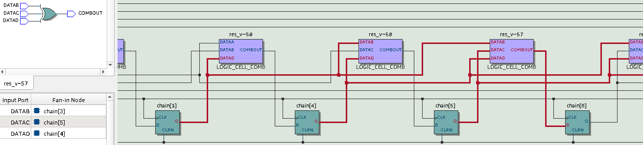
consists of a FF and a LUT. The LUT at chain position i uses the outputs from the three previous FFs to compute the next
value for the cell's FF:
chain(i) <= combine_f(chain(i-3), chain(i-2), chain(i-1));
A logical XOR of all inputs is used as combination function (combine_f()).
Technology view (cut-out, Quartus Prime): computation of next value for register chain[6]
via one LUT by using the states of the previous three registers chain[3], chain[4] and chain[5]
And combining them via XOR:
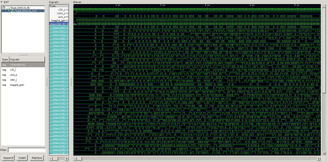
The beginning of the chain use an additional FF, which toggles every clock cycle to "start" the chain. After a short "initialization" time the chain oscillates in a pseudo-random way generating very high chaotic switching activity and dynamic power consumption.
The top entity is rtl/fpga_torture.vhd:
entity fpga_torture is
  generic (
    NUM_CELLS : positive -- number of LUT3+FF elements
  );
  port (
    clk_i  : in  std_ulogic; -- clock input
    rstn_i : in  std_ulogic; -- low-active async reset
    out_o  : out std_ulogic  -- dummy output (LED or unconnected FPGA pin)
  );
end fpga_torture;
The reset signal rstn_i is optional if the target FPGA supports FF initialization via bitstream. In this case the
rstn_i signal can be tied to 1. The out_o output signal is required to prevent the synthesis tool from removing
the whole design logic. Connect this signal to some uncritical FPGA output pin like a LED or an unconnected FPGA pin.
💡 Simulate/test the configuration of NUM_CELLS using the testbench before doing synthesis. Some NUM_CELLS values
(like 32) result in maximum switching activity (all FFs toggling in every cycle).
The projects provides a simple testbench
(sim/fpga_torture_tb.vhd), which
can be simulated by GHDL via the provides script (sim/ghdl.sh):
fpga_torture/sim$ sh ghdl.sh
The simulation will run for 1ms using a 100MHz clock. The waveform data is stored to sim/fpga_torture.vcd
so it can be viewed using gtkwave:
fpga_torture/sim$ gtkwave fpga_torture.vcd
The total size of the chain is defined by the NUM_CELLS generic. The design will require
NUM_CELLS+1 FFs (registers) and NUM_CELLS+2 LUT3s (look-up tables, 3-inputs each). Some
FPGAs/toolchains might also introduce some additional route-through LUTs.
Mapping example: Lattice iCE40UP5K-UWG30ITR FPGA, SinplifyPro, NUM_CELLS = 5278
   Number of slice registers: 5279 out of  5280 (100%)
   Number of I/O registers:      0 out of    63 (0%)
   Number of LUT4s:           5280 out of  5280 (100%)
      Number of logic LUT4s:               5280
      Number of ripple logic:                 0 (0 LUT4s)
   Number of IO sites used:      3 out of    21 (14%)
   Number of Clocks:  1
      Net clk_i_c: 5279 loads, 5279 rising, 0 falling (Driver: Port clk_i)
   Number of LSRs:  1
      Net rstn_i_c_i: 5279 loads, 5279 SLICEs