Getting To Know The Board
This page contains information regarding the original (V1) IOIO boards. For information on the newer IOIO-OTG board, please visit This page.
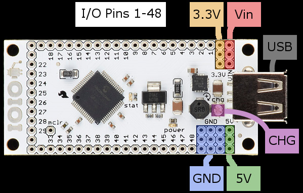
The IOIO board contains the following components:
- USB connector (type A) female connector: Used to connect to the Android device.
- GND pins (9 pins): Ground connection.
- VIN pins (3 pins): Used for power supply to the board. Voltage between 5V-15V should be supplied.
- 5V pins (3 pins): Normally used as 5V output when the board is powered from VIN. Can be used as 5V input in case VIN is not connected.
- 3.3V pins (3 pins): 3.3V output.
- I/O pins (48 pins, numbered 1-48): General purpose I/O pins. Some have special functions, see below.
- power LED: Lights when the IOIO is getting power.
- stat LED: Lights briefly during power-up and then becomes under application control.
- mclr pin: Not normally used. Its purpose is for programming new bootloader firmware on the IOIO board.
- Charge current trimmer (CHG): Adjusts the amount of charge current supplied on the VBUS line of the USB to the Android device. Turning in the (+) direction increases charge current.
The I/O pins are the essence of the IOIO. They are used to connect to external circuits using different interfaces. The common denominator to all pins is that they can all serve as 3.3V digital inputs or 3.3V digital outputs. In addition, many of the pins are capable of other functions as detailed in the table at the bottom of this page.
For convenience, the common pin functions are presented graphically on the bottom of the board, with a legend:
- Pins surrounded by a square can be used as analog inputs (3.3V). For more details, see Analog Input.
- Pins surrounded by a circle are 5V-tolerant, i.e. can be used as 5V logic inputs or product 5V logic output when used in open-drain mode with the help of a pull-up resistor. For more details, see Digital I/O.
- Pins marked with "P" can be used as peripheral inputs and outputs. Mainly, this includes PWM, UART, and SPI.
- The pin marked with "Pi" can be used as peripheral input (but not output).
- Pins marked with DAx and CLx are used for TWI.
Note: Due to an error in the silk screen (text and graphics printed on the board) design of V1.5 (the first batch of commercial boards), the letter "P" has been omitted from the peripheral pins 34-40 and 45-48. Those 11 pins can, however be used as peripheral inputs or outputs.
This table applies to IOIO V1.1 - V1.5 boards.
Specific design files in EAGLE format can be downloaded here.
####Legend:
- A/D: pin can be used as analog input
- I2C: pin can be used as I²C: DAx - data pin if I²C module number x, CLx - clock pin if I²C module number x
- PPSi: pin can be used as input for remappable peripherals (input capture, UART, SPI)
- PPSo: pin can be used as output for remappable peripherals (UART, SPI, comparator output)
- 5V: pin is 5V tolerant: can be used as 5V input or 5V output in open-drain mode
- Comp: pin can be used as comparator input number as specified
- Prog: pin can be used for ICSP: use Vpp and either C1/D1, C2/D2 or C3/D3 which are clock and data, respectively
####Notes:
- All pins can be used as digital input / output (GPIO)
- All pins can be used as “interrupt on change”
| IOIO pin | A/D | I²C | PPSi | PPSo | 5V | Comp. | Prog. | PIC pin | PIC function |
|---|---|---|---|---|---|---|---|---|---|
| 1 | 39 | OSCI/CLKI/CN23/RC12 | |||||||
| 2 | 40 | OSCO/CLKO/CN22/RC15 | |||||||
| 3 | Y | Y | Y | 42 | RTCC/DMLN/RP2/CN53/RD8 | ||||
| 4 | DA0 | Y | Y | Y | 43 | DPLN/SDA1/RP4/GD8/CN54/RD9 | |||
| 5 | CL0 | Y | Y | Y | 44 | SCL1/RP3/GD6/CN55/RD10 | |||
| 6 | Y | Y | Y | 45 | RP12/GD7/CN56/RD11 | ||||
| 7 | Y | Y | Y | 46 | DMH/RP11/INT0/CN49/RD0 | ||||
| 8 | 3D | 47 | SOSCI/C3IND/CN1/RC13 | ||||||
| 9 | Y | 3C | 48 | SOSCO/SCLKI/T1CK/C3INC/RPI37/CN0/RC14 | |||||
| 10 | Y | Y | Y | 49 | VCPCON/RP24/GD9/VBUSCHG/CN50/RD1 | ||||
| 11 | Y | Y | Y | 50 | DPH/RP23/CN51/RD2 | ||||
| 12 | Y | Y | Y | 51 | RP22/GEN/CN52/RD3 | ||||
| 13 | Y | Y | Y | 52 | RP25/GCLK/CN13/RD4 | ||||
| 14 | Y | Y | Y | 53 | RP20/GPWR/CN14/RD5 | ||||
| 15 | 3B | 54 | C3INB/CN15/RD6 | ||||||
| 16 | 3A | 55 | C3INA/SESSEND/CN16/RD7 | ||||||
| 17 | 58 | GD10/VBUSST/VCMPST1/VBUSVLD/CN68/RF0 | |||||||
| 18 | Y | 59 | GD11/VCMPST2/SESSVLD/CN69/RF1 | ||||||
| 19 | Y | 60 | GD0/CN58/RE0 | ||||||
| 20 | Y | 61 | GD1/CN59/RE1 | ||||||
| 21 | Y | 62 | GD2/CN60/RE2 | ||||||
| 22 | Y | 63 | GD3/CN61/RE3 | ||||||
| 23 | Y | 64 | HSYNC/CN62/RE4 | ||||||
| 24 | Y | 1 | VSYNC/CN63/RE5 | ||||||
| 25 | CL2 | Y | 2 | GD12/SCL3/CN64/RE6 | |||||
| 26 | DA2 | Y | 3 | GD13/SDA3/CN65/RE7 | |||||
| 27 | Y | Y | 1D | 4 | C1IND/RP21/CN8/RG6 | ||||
| 28 | Y | Y | 1C | 5 | C1INC/RP26/CN9/RG7 | ||||
| 29 | Y | Y | 2D | 6 | C2IND/RP19/GD14/CN10/RG8 | ||||
| 30 | Y | Y | 2C | 8 | C2INC/RP27/GD15/CN11/RG9 | ||||
| 31 | Y | Y | Y | 1A | C3 | 11 | PGEC3/AN5/C1INA/VBUSON/RP18/CN7/RB5 | ||
| 32 | Y | Y | Y | 1B | D3 | 12 | PGED3/AN4/C1INB/USBOEN/RP28/CN6/RB4 | ||
| 33 | Y | 2A | 13 | AN3/C2INA/VPIO/CN5/RB3 | |||||
| 34 | Y | Y | Y | 2B | 14 | AN2/C2INB/VMIO/RP13/CN4/RB2 | |||
| 35 | Y (ref +) | Y | Y | C1 | 15 | PGEC1/AN1/VREF-/RP1/CN3/RB1 | |||
| 36 | Y (ref -) | Y | Y | D1 | 16 | PGED1/AN0/VREF+/RP0/CN2/RB0 | |||
| 37 | Y | Y | Y | C2 | 17 | PGEC2/AN6/RP6/CN24/RB6 | |||
| 38 | Y | Y | Y | D2 | 18 | PGED2/AN7/RP7/RCV/CN25/RB7 | |||
| 39 | Y | Y | Y | 21 | AN8/RP8/CN26/RB8 | ||||
| 40 | Y | Y | Y | 22 | AN9/RP9/CN27/RB9 | ||||
| 41 | Y | 23 | TMS/CVREF/AN10/CN28/RB10 | ||||||
| 42 | Y | 24 | TDO/AN11/CN29/RB11 | ||||||
| 43 | Y | 27 | TCK/AN12/CTEDG2/CN30/RB12 | ||||||
| 44 | Y | 28 | TDI/AN13/CTEDG1/CN31/RB13 | ||||||
| 45 | Y | Y | Y | 29 | AN14/CTPLS/RP14/CN32/RB14 | ||||
| 46 | Y | Y | Y | 30 | AN15/RP29/REFO/CN12/RB15 | ||||
| 47 | DA1 | Y | Y | Y | 31 | SDA2/RP10/GD4/CN17/RF4 | |||
| 48 | CL1 | Y | Y | Y | 32 | SCL2/RP17/GD5/CN18/RF5 | |||
| stat LED | Y | Y | Y | 33 | RP16/USBID/CN71/RF3 | ||||
| mclr | Vpp | 7 | MCLR |