Timings
This section is focused on specifics about how the timings in the execution of the instructions of the SSP1601 DSP within the SVP chip work.
To this day this seems to be the area with more gaps in knowledge regarding the SVP. The general behavior of Virtua Racing contains lots of synchronization with the Motorola 68000 side, making detailed timing knowledge not really required to correctly emulate the game. Most emulators treat all instructions as running at the same speed, and a general figure of 7-8 MIPS in the DSP execution was measured to be just enough to run the game without issues.
On its own, the DSP inside the SVP chip can address 64 KWords of code, that can be run from three different sources:
- External ROM: the main source of code and data in the Virtua Racing cartridge, an external 2MB/16bit ROM chip with access times of probably 120ns (note: this is unconfirmed, but prototype cartridges used four 8-bit 120ns EPROMs - in my current experiments a 100ns EPROM works just fine). Code and data from this source is addressed from 0x0400 to 0xFBFF.
- IRAM: a writable memory of 1 KWord. Set up to be dynamically filled with routines that are used more often or require a faster access time. This area is addressed from 0x0000 to 0x03FF.
- IROM: a 1 KWord internal ROM containing the boot code for the SVP chip as well as routines intended to be used often in games. It also contains the 4 interrupt vectors for the DSP. Addressed from 0xFC00 to 0xFFFF.
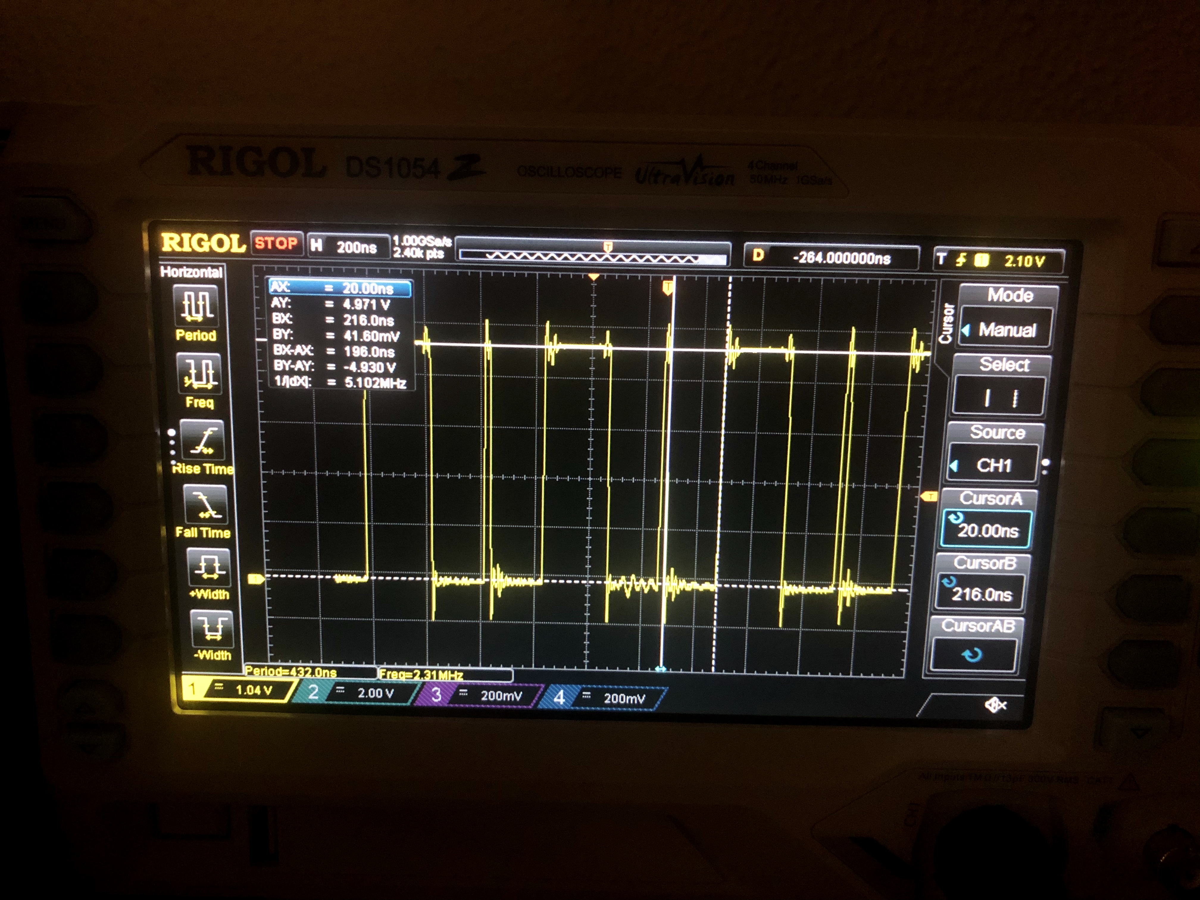
Basic instruction cycle timings were measured using an oscilloscope. All the following timings were based on the MPYA instruction that, according to the SSP1601 datasheet, takes a single instruction cycle to execute. Routines that executed the same instructions over and over were used to measure the timings when running over ROM, while a different approach was used for IRAM instructions (i.e.: running a definite set of instructions on IRAM, then going back to ROM space and compare timings). The following values were found:
- ROM: 216ns.
- IRAM: ~44ns (see note below).
- IROM: assumed to be the same as IRAM (see following sub-section "Real-life situation").
Note: IRAM timings seemed variable, running 3 instructions took 53ns each, while 16 instructions took 45ns each and 64 took 43.75ns. Probably the jump from IRAM to ROM space had an overhead that influenced more in the former case than the latter. Also note that the latter figure closely matches the assumed 23MHz frequency that's assumed for the DSP inside the SVP chip.
My first approach to measure the different timings was to run the following test routine from the internal ROM (one that performs fixed-point addition) over and over for a set period of time controlled by the Mega Drive side of things. After 250 frames (5 seconds in an European console) these were the results:
| Source | Executions (5s) |
|---|---|
| ROM | 426864 |
| IRAM | 626265 |
| IROM | 626265 |
Values varied slightly among multiple runs, values in table averaged
This shows that on a "real-life situation" (mixed ROM/IRAM code, loads to/from DRAM, accesses to ROM from MegaDrive, etc...) code run from the IRAM (or routines within the IROM) run at a 146% speed than code accessed from the external ROM.
Note: this section is based on guess-work on the currently known behavior of the chip
It makes sense that code runs slower while the SVP chip accesses an external resource. Also, the IRAM is internal to the DSP and the IROM isn't only inside the chip but also is an order of magnitude smaller so they probably could use faster ROM memory for that resource.
Details on how the SVP chip feeds code to the SVP are unknown, but my current guess is as follows: the DSP accesses code through circuitry that acts as a ROM adapter. Based on the requested address, the ROM adapter reaches the IROM area inside the chip or the external ROM chip (IRAM accesses are always internal to the DSP). Knowing that the external ROM is limited on access time, on each access to it, the ROM adapter triggers the SS line on the DSP, effectively stopping the DSP until the ROM chip is ready to provide the requested data.
(This SS line is probably also tied to the 0xA15008 register in the MD area that seems to stop the SVP chip at some points during Virtua Racing operation - will research on this at some point).
AFAIK, emulators aren't discriminating between these sources timing-wise. They also seem to deal with instruction timings by treating them all as one-cycle instructions.
That being said, as MiSTer's emulation relies on two different memories within the DE-Nano10 board for the emulation to work (BRAM is used for the internal memories and IRAM, SDRAM for the ROM), it had pretty close rates of timing differences between IRAM and ROM accesses (IRAM was 78% faster than the ROM - based on running the previously mentioned test program on it). But it ran 2.3-2.5x faster than the real hardware).
The SVP chip seems to relay on a clock based on the VCLK signal from the cartridge input. At the top part of the chip there's a small RC circuit based on three resistors (R1, R2 and R3) and three capacitors (C12, C13 and C14) that could work as a PLL based on VCLK. The output of that circuit seems to be C12, which outputs a clock signal of around 46MHz (45.6MHz - measured on a PAL cartridge running at 50Hz.).
Tests by user Jorge@Plutiedev showed that this clock signal changes in different systems (i.e.: a cartridge dumper outputting a lower frequency in VCLK pin). Note that this was measured on European Virtua Racing cartridges, and JP/US carts could behave differently.
This approach would allow for synchronization between accesses from the DSP and the 68000 to the external ROM.
Note: currently work in progress - will take some time until this is complete
The goal of this section is to determine how each instruction takes to read/execute compared to the others. Only accesses to the external ROM are taken into account, as it's impossible to access the IROM or IRAM (being within the chip). But with accurate figures for each instruction, more or less accurate timings can be inferred taking into account the measures that can be found in the previous section.
The following figures were obtained by checking timings of accesses from the SVP chip to the EPROM running a simple code that repeats the same instruction continuously, like:
# Speed test for individual instructions

org 0400

test_init:
            mpya (r4), (r0)
            bra always, @test_init
At the Mega Drive side of things, execution of instructions in the M68000 side is halted by running:
stop #2700
Thus disabling all interrupts and effectively halting the CPU. At that moment, the SVP is the only component reading code from the EPROM, leading to readings in the oscilloscope as follows:
Note: according to the SSP1601 datasheet, MPYA is run in a single instruction-cycle, so I'll be basing the comparisons on the timings of that instruction.
Note 2: these numbers are purposedly ignoring accesses from the 68000 side to the ROM.
Note 3: these were measured by hand so they're not to be taken 100% accurate, more like a measure of how the DSP behaves within the SVP chip and if there are differences in how each instruction runs.
Note 4: not all combinations have been tested. i.e.: conditional branching has been tested and results in no cycle increases in branching, so it's assumed to happen this way in all instructions that allow it.
One execution cycle (executed in ROM) seems to equal 216 ns, while in IRAM seems close to 45 ns.
| Instruction | Words | Cycles | Notes |
|---|---|---|---|
| MPYA (rY), (rX) | 1 | 1 | |
| BRA [cond], addr | 2 | 2 | |
| LD rX, imm | 1 | 1 | |
| LD (rX), imm | 2 | 2 | |
| LD RAM[addr], a | 1 | 1 | i.e.: LD A[0x00], a / LD B[0x00], a |
| LD A, ((rX)) | 1 | 3 | See "Timing quirks" section - point 2 |
| OP A, (rX+) | 1 | 1 | ALU op, operand in RAM, with address modifier |
| OP A, ((rX)) | 1 | 3 | ALU op, operand in ROM |
| MOD [cond], op | 1 | 1 |
Whenever the DSP tries to bring one of the address lines up or down and it's already at that value (i.e.: 0->0 or 1->1), a short burst of the oposite value can be seen for around 24ns (i.e.: 0->0, a short 1 voltage appears for 24ns. I'm taking these into account while measuring the different instructions as it seems to be part of the normal behavior of the ROM adapter inside the DSP.
During the research of these timings, there came up evidences of a basic pipeline execution within the DSP (something that's common in DSPs anyways). Rollback behavior consistent with this is described next.
Some instructions allow the DSP to read data from ROM directly and copy it to the accumulator register. When that happens, the DSP has to go to the ROM and ask for that data. Take a look at the following routine:
org 0400

test_init:
            ld r0, 0x00
            ld (r0), 0x0408
            ld a, ((r0))        # read ROM data from address 0x0408 into register A
test_loop:  bra always, @test_init
While running this infinite loop, the following timings were measured from the access of the SVP to the EPROM holding the code:
| Address (last 4 bits) | Opcode | Read time (ns) |
|---|---|---|
| 0000 | ld r0, 0x00 | 216 |
| 0001 | ld (r0), ... | 216 |
| 0010 | ld (r0), 0x0408 | 216 |
| 0011 | ld a, ((r0)) | 216 |
| 0100 | bra always,... | 216 |
| 1000 | data from 0x408 | 216 |
| 0100 | bra always,... | 220 |
| 0101 | bra always, 0x0400 | 216 |
| 0000 | ld r0, 0x00 | 216 |
Notice how after executing ld a, ((r0)), instead of going right ahead to get the data in 0x0408, instead it jumps to the location of the following instruction. Then, at the next 216ns cycle, it goes to 0x0408 to grab the requested data. After that goes back to the following instruction and perform its first read for a second time, suggesting there was some kind of rollback mechanism at play here.
This suggests that a basic pipeline process is happening within the DSP, so while the first instruction word from 0100 was retrieved the instruction read before was being executed. And after executing it, the processor halted the current instruction read and went back to retrieve the requested data from 0x0408 (last four bits 1000). Then it went back to continue reading the following instruction (and seemingly having discarded the previously retrieved instruction word, thus "wasting" an extra execution cycle).
The same behavior happens while reading from IRAM, but the whole process happens faster:
| Address (last 4 bits) | Opcode | Read time (ns) |
|---|---|---|
| 0000 | ld r0, 0x00 | 216 |
| 0001 | ld (r0), ... | 216 |
| 0010 | ld (r0), 0x0308 | 216 |
| 0011 | ld a, ((r0)) | 216 |
| 0100 | bra always,... | 216 |
| xxxx | gap - IRAM read | ~30 |
| 0100 | bra always,... | 216 |
| 0101 | bra always, 0x0400 | 216 |
| 0000 | ld r0, 0x00 | 216 |
During IRAM access some address lines went high on their own, but not pointing to any valid value in particular. This whole "burst" lasted 70ns.
Notice that this behavior happens everytime that ROM/IRAM is read as data, independently of whatever the next instruction is. That means that this probably is done to allow RAM inside the DSP to refresh before the next instruction is run (as every read on ROM/IRAM involves a pointer within RAM that's auto-incremented after each access).
Note: this is consistent with CD2450's behavior. It also takes 3 clock cycles to read directly from PRAM (it also takes 4 cycles to write into PRAM, something the SSP1601 can't do)