SVP decap and details
Except where noted, all provided images were made by Richard Kaussler from Richi's Lab. More details on the internal structures from the SVP die can be found in its incredibly detailed post about it. I just provided the victim chip :)).
This article is meant as a repository of the amazing pictures taken by Richard, and also to offer some commentary on the details he's found on the chip from a programmer's point of view. As mentioned before, the more technical side of how the die is configured is already covered by him. In some cases I'll offer some corrections on details I think might be off, but just from my point of view and the (limited) experience I have working with the SVP chip.
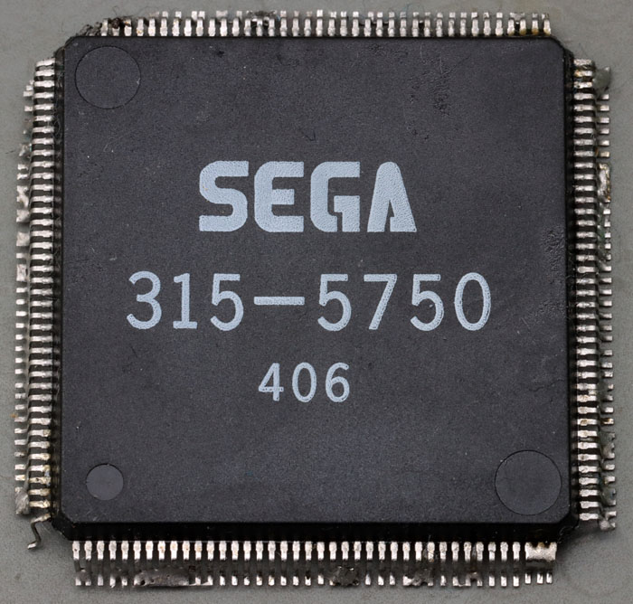
Anyone who has opened a Virtua Racing cartridge has found the glorious sight of the large SVP chip in the middle of its PCB. Usually covered by thermal paste, once removed it shows the following internal number on its top: SEGA 315-5750.
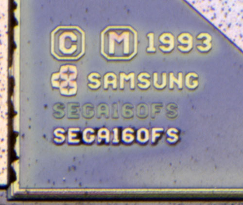
Internally, the SVP chip was known as SEGA160FS, a designator already found in internal SVP dev cartridges sold online, as well as in the upper right corner on the die. Not sure what the FS suffix means, but the 160 hints to the chip clearly being a Samsung DSP from the SSP160x series.
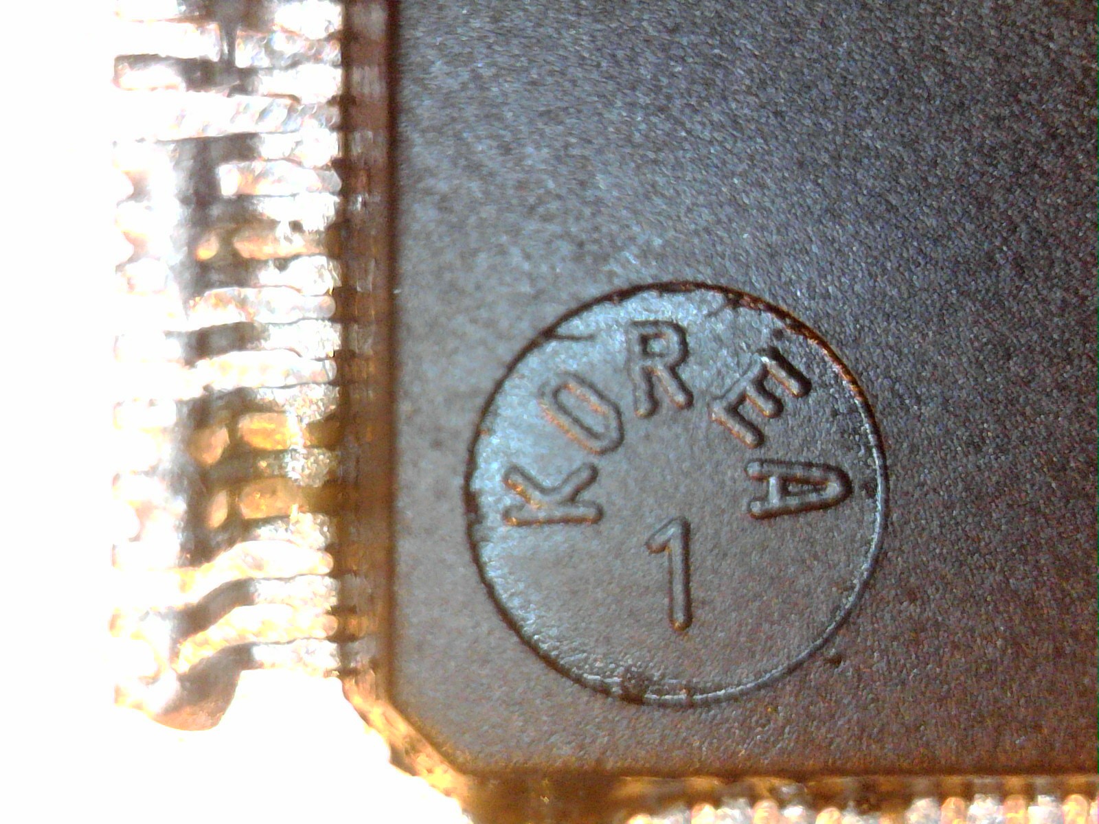
The SVP also seems to have been manufactured in South Korea.
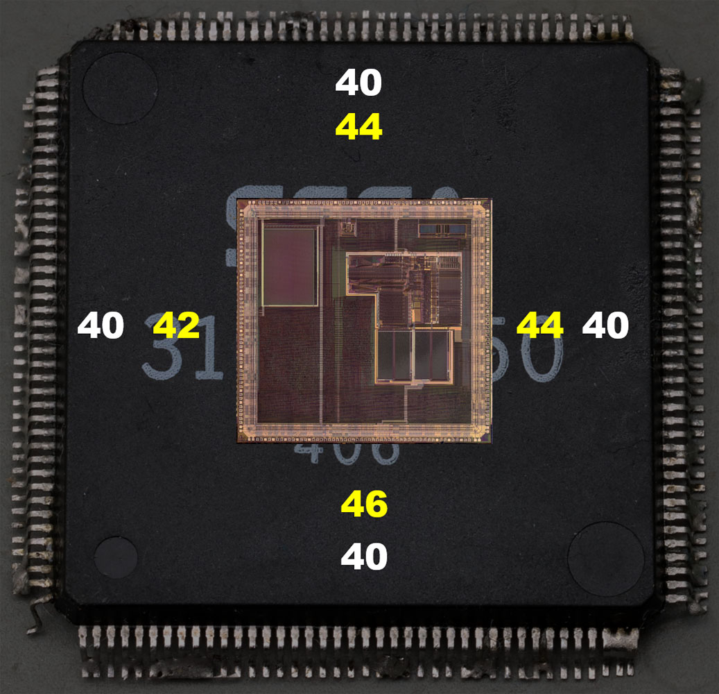
The chip comes in a TQFP package with 120 pins. Here's a comparison of the size of the internal die compared to the chunky package:
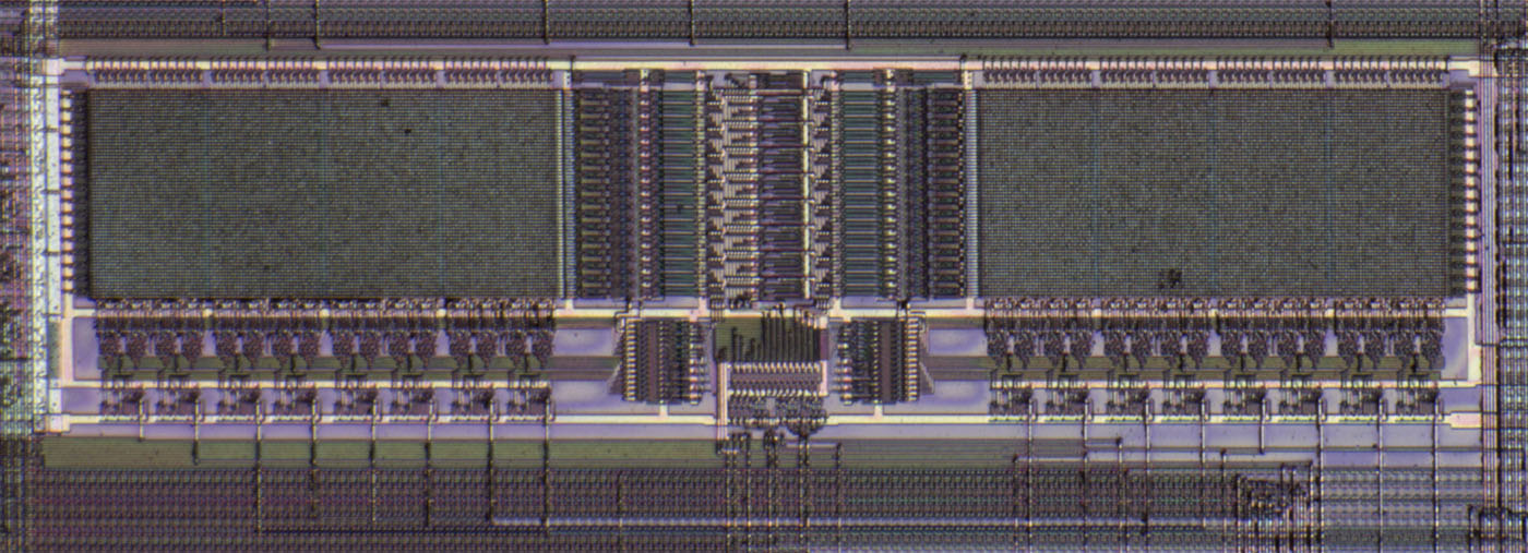
A more general view of the chip internals can be seen here:
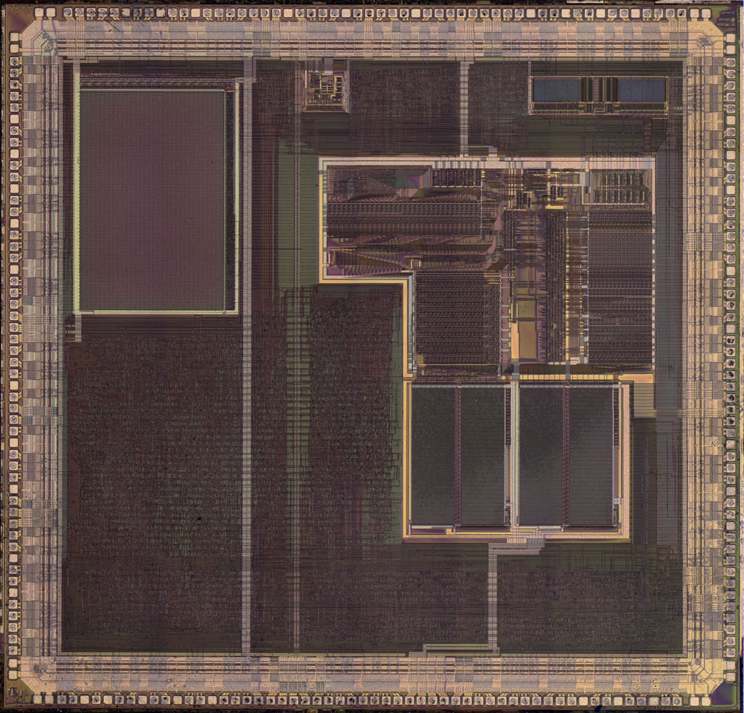
You can also find the full hi-res (15632x16312, 57.8MB) version of this picture https://raw.githubusercontent.com/jdesiloniz/svpdev/master/img/decap/full_decap.jpg.
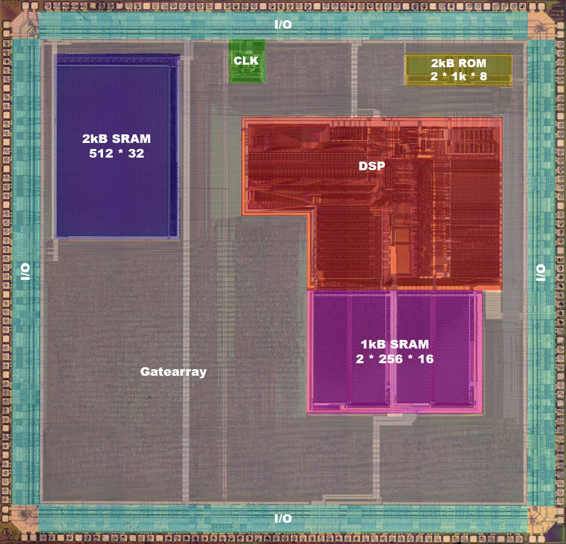
On the upper center part of the die there's a small area dedicated to generating the clock signal for the DSP (and possibly other components). It contains rather big components compared to the rest of the internal blocks. It's connected to the RC circuit in the top of the cartridge which, combined with this circuit, generates a multiplied signal from the internal M68000 clock coming from the cartridge port. This circuit possibly allows this and divides the signal to provide the final ~23MHz clock fed to the DSP. More information about the internal timing can be found here.
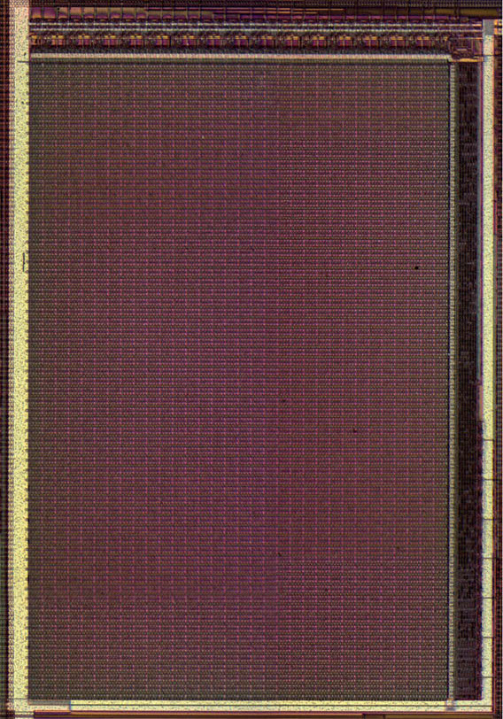
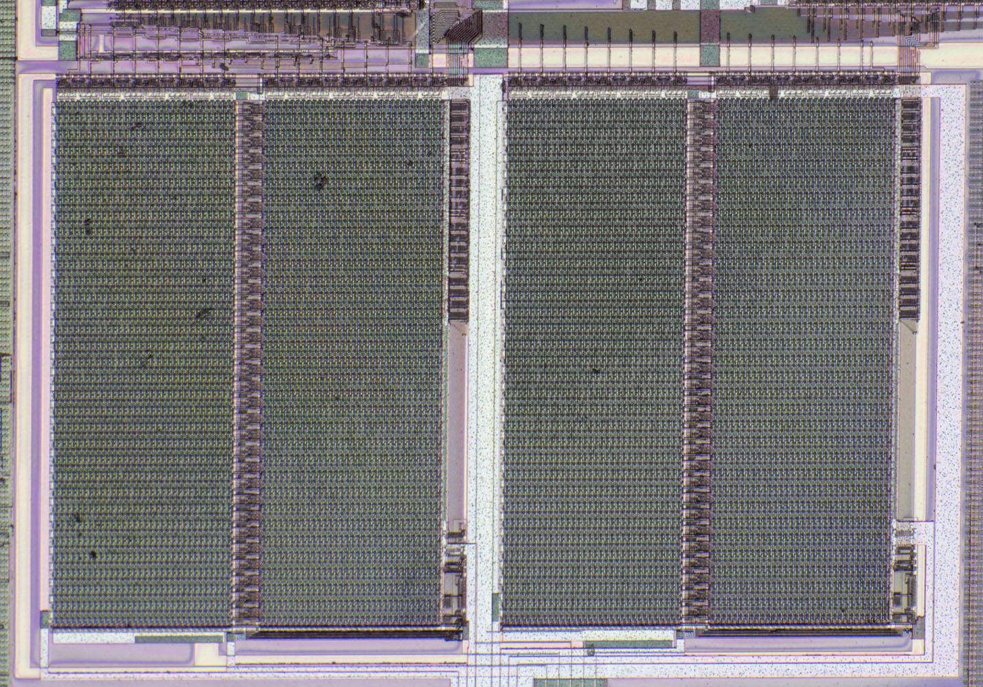
The SSP1601S DSP allows users to configure the DSP to run code from either ROM or RAM memories. In the case of the SVP, a 2KB SRAM exists inside the chip being, by far, the widest component inside the chip. Developers can dynamically load routines onto the IRAM which allows the DSP to run code on a quite faster speed than from the external ROM (3x times faster). Virtua Racing does this extensively, both in its internal ROM and its test routines.
For some reason the IRAM area is less dense than the RAM blocks attached to the DSP. Richard has mentioned this but he's not sure the reason for it.
As was already found from running code inside the chip in 2021, the SVP has an internal ROM that contains a boot-up process that ends up pointing the DSP to the right part of the cartridge to start running the game, as well as a (completely unused) 3D graphics library.
It strikes how small the 2KB ROM is, compared to the aforementioned IRAM. Richard's pictures also allowed to confirm that there's no additional ROM inside the cartridge (that could have been activated with some unknown behavior of the external registers).
A higher resolution version of this picture can be found here.
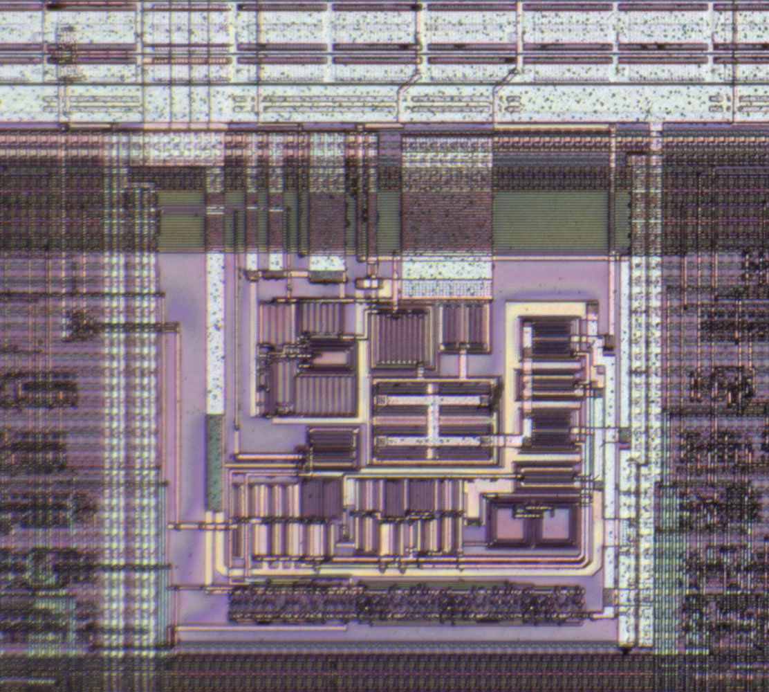
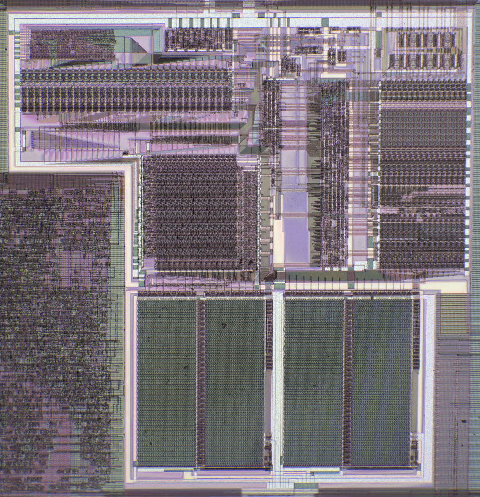
Here's the main component of the SVP chip: Samsung's SSP1601S. There was another variant, the SSP1601M, which differs in some areas (e.g.: in some samples found in Samsung's website years ago, interrupt vectors were put at the beginning of ROM space for M type DSPs, while the SSP1601S do it at the end of ROM space like it's the case in the SVP). SSP1601 stands for "Samsung Signal Processor - 16 bit - DSP core 01".
Main areas of interest are its ALU, multiplier and internal RAM blocks.
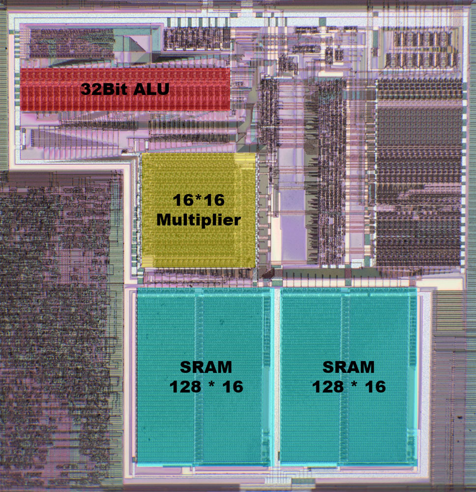
Here we can see the 32-bit DSP ALU in all its glory. Apparently each 32 bit is handled in one of these columns, allowing for the already known operations: addition, substraction, logic and, logic or, logic xor, and comparison.
The main component in the DSP is its 16x16 multiplier. You can also see how it connects to the ALU, probably to allow for the MPYA (multiply and add) and MPYS (multiply and substract) operations.
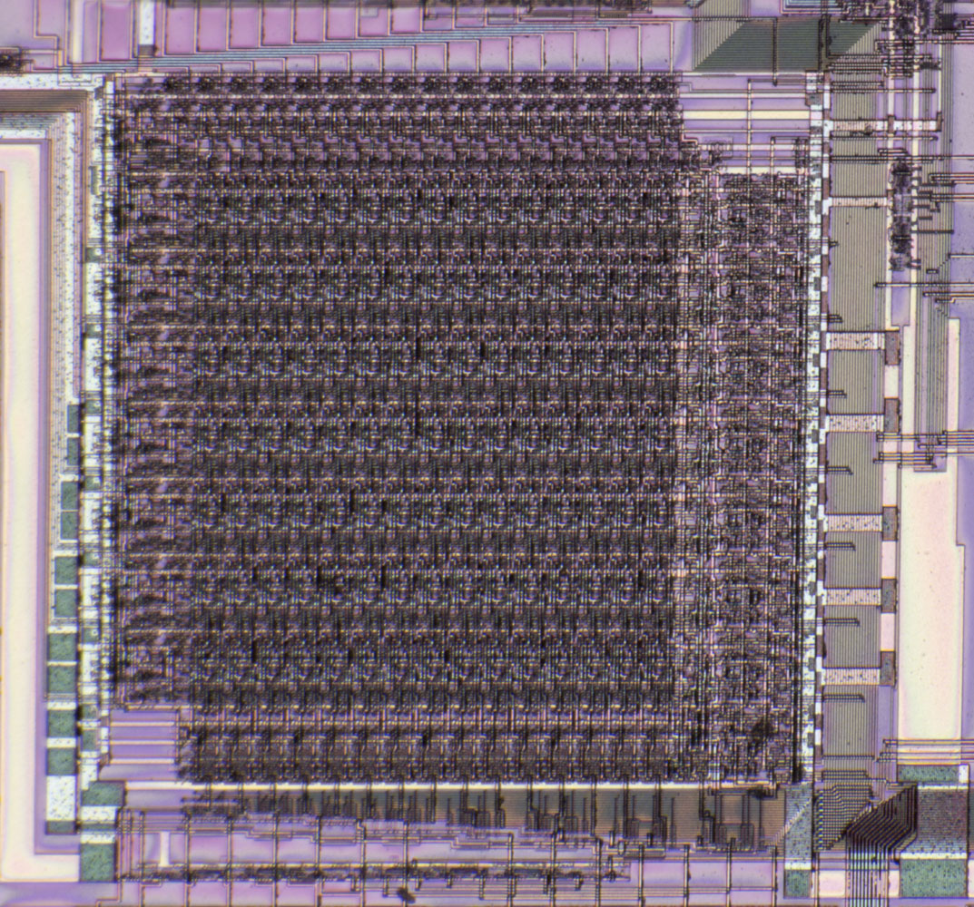
Finally, the two internal 256 word RAM blocks (RAM0 and RAM1) can be seen here too, closely tangled to the DSP to allow for one-cycle updates on them (also showing that these weren't optional, as opposed to the IRAM).
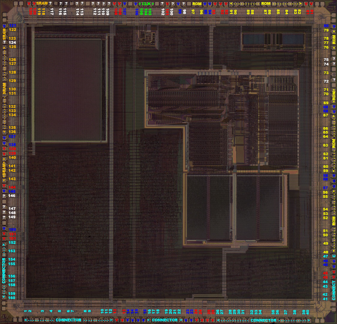
Richard was kind enough to track down each individual pin to the bounding wires inside the die. More details can be found on his website. One detail that really called my attention is how there are unknown logic pins in the pinout (pins 72,74,75 and pins 109-117, unconnected or left to 5V and GND in the final version of the cartridge). Being near the area where the SDRAM/ROM control pins are, my gut feeling is that these were used to allow for different memory types, or probably for an external RAM emulator during the development process. For the ROM ones, the devkits allowed for SCSI ROM emulation so those might be used for that purpose.
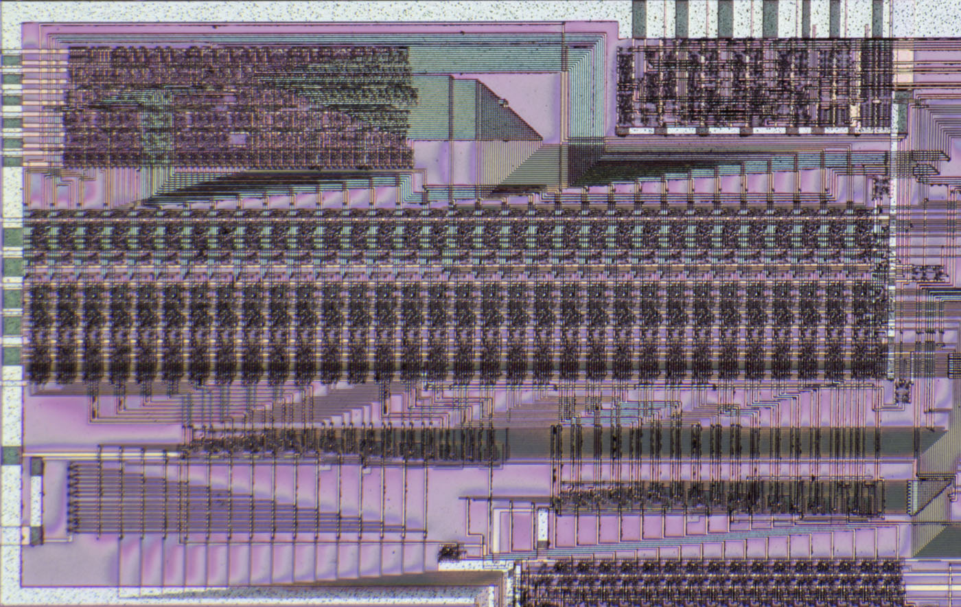
The detail of this pictures is astounding, but more resolution would be required to be able to tell apart some of the internal circuitry that can't be really be identified. Most of the gate array that hasn't been identified probably deals with:
- Responding properly to the cart connector signals
- Inter-block connections
- External registers and other custom circuitry.
- Interrupt generation.
As mentioned before, some of the SEGA custom circuitry is partially or completely unknown and probably buried in that sea of gates :(. Will update this section in case more details can be found.