There are better tools to create artistic pcb here is one that i recommend: https://github.com/wntrblm/Gingerbread
Inkscape extension for exporting drawings into a KiCad PCB.
- Draw Any kind of shapes without restriction
- Supports Drill Pad, and custom drill size
- Supports Edge Cut (PCB Shape)
- Works on OSX, Windows and Linux
Warning: starting from 0.2.18 svg2shenzhen only support Inkscape 1.0 and above
- Download the latest version (0.2.18.7)
- Windows https://github.com/badgeek/svg2shenzhen/releases/download/0.2.18.7/svg2shenzhen-extension-0.2.18.7.zip
- Linux / OSX https://github.com/badgeek/svg2shenzhen/releases/download/0.2.18.7/svg2shenzhen-extension-0.2.18.7.tar.gz
- Release notes: https://github.com/badgeek/svg2shenzhen/releases
- Older version: https://github.com/badgeek/svg2shenzhen/releases
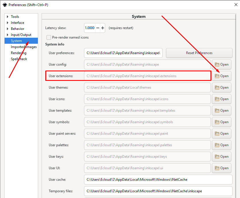
- Extract and copy the files into the directory indicated in Inkscape under Edit -> Preferences -> System: User extensions
Step by Step Guide with Screenshot
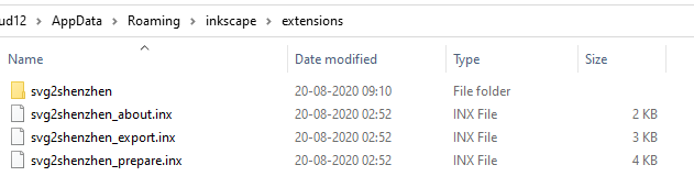
- Go to your extracted folder it should look like this
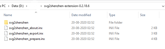
- Copy all files ("svg2shenzhen" folder + svg2shenzhen_about.inx + svg2shenzhen_export.inx + svg2shenzhen_prepare.inx)
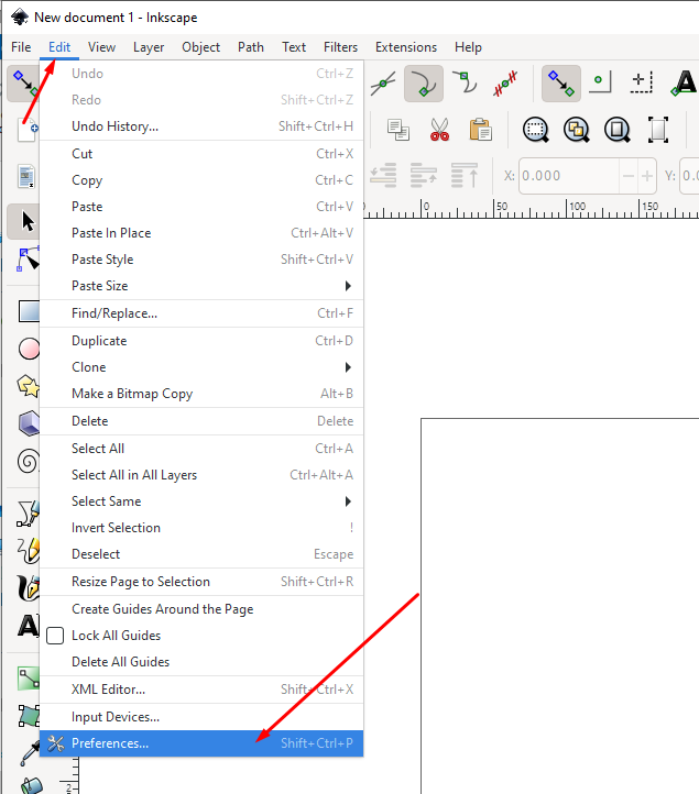
- Open Inkscape and go Edit --> Preferences
- Under Preferences go to System, Now in System info you will see option User extensions: this is the path of extension. You can hit on Open icon and it will open up the folder.
- Paste all the files copied
- Restart Inkscape
In Inkscape:
- Extension > Svg2Shenzhen > Prepare Document
- Choose layer (F.Cu.. etc)
- Draw PCB
- Extension > Svg2Shenzhen > Export KiCad
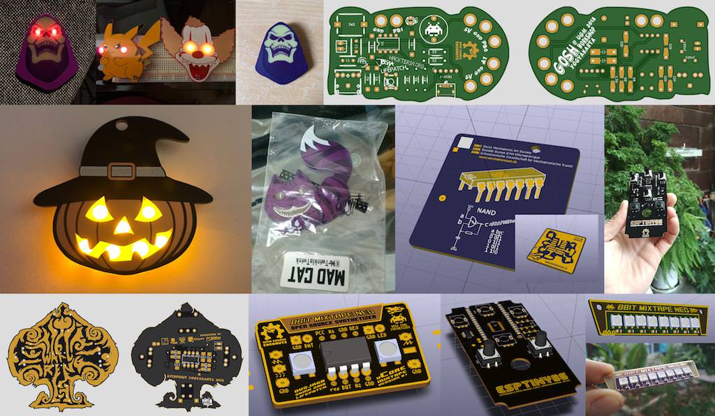
Download and open Example PCB
- Custom Footprints for KiCad - https://www.gabetaubman.com/blog/posts/kicad-custom-footprint/
- PCBArt Badge - http://blog.sheasilverman.com/2019/01/pcbart/
- After the Prepare Document step, only two fabrication layers are used: Edge.Cuts and Drill, and for the different PCB-layers, only the F.Cu layer is active. The others have the post-fix "-disabled" in their layer name; change this by removing this post-fix to enable more layers.
- Special use of the solder-mask layers F.Mask and B.Mask: Due to the fabrication standard of PCB manufacturing, when enabled, this will lead to the solder-mask NOT being present where there are black areas in your design. This is kinda PCB/KiCad standard, but can be confusing. If you want to Get-What-You-See from Inkscape, meaning that you really draw the color where you want the solder-mask to be, change the layer name to F.Mask-invert
- Super easy simple PCB with exposed copper surrounded by solder-mask, can be generated automatically by leaving the F.Mask layer empty and renaming it to F.Mask-auto.
- Feel free to add your own layers, for testing graphics and designing stuff. All these other layers will be ignored.
- For Edge.Cut layers, you need to convert any polygons or objects to paths with only an outline, no fill. Don't use any groups on Edge.Cut layers, and if you have paths with inner cut-outs, break them apart into separate paths.
- For Drill layers, place circle objects, and they will be converted into drill pads in KiCad with the same diameter. These drills will not have annular rings, unless you also add copper to the F.Cu and B.Cu layers. Don't use any groups on the Drill layer either.
- Svg2Shenzhen Announcement on Gosh Community Forum
- PCB Art with Inkscape - Developer log on the 8BitMixtape Wiki
- Practical Guide to Designing PCB Art
- KitSprint ANORG 2018
- Drawing PCBs with Inkscape (FOSSDEM) with @kasbah of kitspace - https://www.youtube.com/watch?v=xXRPw7ItMaM
- Making a PCB Badge for Hackaday Supercon! - https://www.youtube.com/watch?v=YqdBiOj8uXw
- Understanding and Making PCB Art (mrtwinkletwinkle) https://www.youtube.com/watch?v=Sbkvza8cKQE
This project is developed independently and without any connection to funding or big collective or organization. Donation is highly appreciated. Go to https://www.patreon.com/badgeek to become a patron and support this project

- inkscape-export-layers - https://github.com/jespino/inkscape-export-layers
- bitmap2component (kicad) - https://github.com/KiCad/kicad-source-mirror/tree/master/bitmap2component
- csv_output - https://github.com/tbekolay/csv_output
- svg2mod - https://github.com/svg2mod/svg2mod