The Instructions
Professor Ken Arnold's instruction video
This assignment is to create two state machine designs in Verilog and demonstrate them on the FPGA board:
-
Tx: The simpler of the two. When an 8 bit value is loaded into a register using the 8 DIP switches for the number and a push button for the "load" signal, it shifts the byte out in asynchronous serial format (initially at 9600 bits per second, later at an arbitrary, programmable data rate). That begins with a start bit (0), followed by the 8 data bits LSB first, and a stop (1) bit.
-
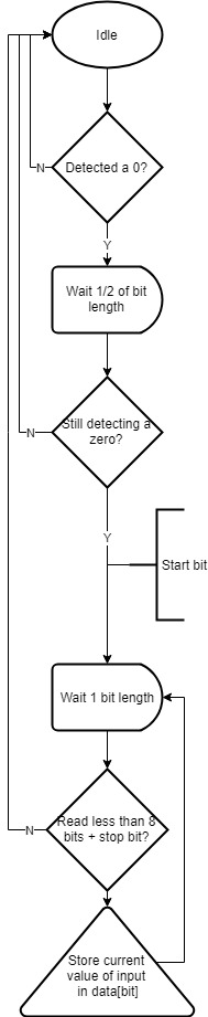
Rx: The tough one, receiving a byte in the format above and displaying it using the LEDs. Your Rx will have to detect the start bit, with 1/2 bit period to confirm a valid start bit, then sample in the middle of each bit interval shifting each bit into an 8 bit register that drives the 8 LEDs on the IO board.
Part 1 - Transmit
For this specific assignment, in part 1 you must implement a UART that takes parallel input data from the switches and buttons, and produces a serial output on one of the FPGA output pins. In order to do that, you must also create a clock with an appropriate frequency to operate the UART from the on-board oscillator connected to the FPGA. The clock frequency should be higher than the data rate to allow for the requirements for part 2 below, most UARTs use a clock that is 16x the data rate. Capture the serial output data on the scope or logic analyzer and confirm the serial output data is correct and that the bit period is 1/9600th second long.**Part 2 - Receive**
In part 2, you will design a serial to parallel receiver that will receive the asynchronous data from your transmitter in part 1 above, and convert it into an 8 bit parallel word for display on the LEDs on the I/O board.Ultimately, you will be implementing the core subset of transmit/receive functions of a device similar to the SCC2691 serial UART chip in the file listed below, (Note: no such file was found in the professor's lab instructions.) so you should review the transmit buffer empty and receive buffer full status registers of that device. For full credit, your final UART design should implement the receive buffer full and transmit buffer empty bits. You will need to take the raw FPGA input clock (8MHz for the older version of the board, 50MHz for the newer rev A board that has DIYchips.com written in white letters on the top of the board) (This instruction was originally written by the teacher with the FPGADEVS6 board from DIYchips.com in mind. This project has been implemented instead on the Digilent Basys 3 which has a single 100 MHz oscillator.) and convert that clock into an appropriate clock for your two state machines.
The Logic
Progress and Conclusions
Progress: I was able to demonstrate Tx using the scope at 9600 baud, as well as Rx displayed using the 8 LEDs. I did not attempt to go any further by adding extra features such as a programmable baud rate.Conclusion: Once I got the UART Tx lab done, the Rx lab was actually surprisingly easy in comparison. If I had more time, I would attempt to add programmable baud rate generation to the Tx and Rx modules.