toc: true title : "Binary Calculator on bare-metal Raspberry Pi 4" date: "February 2020" author: "Augello Andrea, Università degli Studi di Palermo"
\pagebreak
The Embedded System course at Università degli Studi di Palermo requires each student to develop a working and documented embedded application as a final project, which is to be thoroughly discussed during the oral exam.
The course deals with:
- Embedded systems architectures
- Sensors and actuators
- Embedded processors
- Memory architectures
- Input and output
- Multitasking
- Scheduling
- Buses
- Machine language and assembly (ARM)
- Integer and floating-point arithmetics
- Vectored instructions
- Multimedia extension
- Data processing instructions
- Condition flags
- Jumps
- Selection constructs
- Loops
- Memory operations
- Subroutine calls
- Stack handling
- BCM2835/7 Architecture
- STM32-F446 architecture
- Forth
The aim of the course is for the student to know the necessary advanced concepts to the comprehension of the structure of embedded elaboration systems. And also have deep knowledge of embedded system programming.
The following discussion describes the aim, structure, behavior, and usage of the developed system. It also reports the design and implementation choices made during every development phase.
The hardware section briefly describes what components will be used in this project and the rationale behind some of those choices.
The environment section outlines the characteristics of the software tools used to load and run the code.
The software section will describe the developed modules and the decision-making process that brought to their finalized form.
Finally, the conclusion section will sum up the contents of this report and present some possible directions for future improvements to this project.
\pagebreak

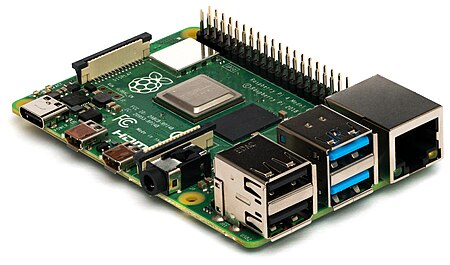
The target for this project is a general-purpose Single-Board Computer: the Raspberry Pi 4 B [Fig. \ref{pi4}].
It is the latest iteration of the Raspberry Pi SoC, launched on 24th June 2019[@PI_release],
it replaces the older Raspberry Pi 3 B+ which was based on the Broadcom BCM2837 chip[@BCM2835][@BCM2835_datasheet_errata] and boasts high-end specs:
- A 1.5GHz quad-core 64-bit ARM Cortex-A72 CPU
- 1GB, 2GB, or 4GB of LPDDR4 SDRAM
- Full-throughput Gigabit Ethernet
- Dual-band 802.11ac wireless networking
- Bluetooth 5.0
- Two USB 3.0 and two USB 2.0 ports
- Dual monitor support, at resolutions up to 4K
- VideoCore VI graphics, supporting OpenGL ES 3.x
- 4Kp60 hardware decode of HEVC video
- Complete compatibility with earlier Raspberry Pi products
Although claiming complete backward compatibility with earlier products, the documentation available[@pi4_datasheet] is not very comprehensive, which makes porting code not always straightforward.
The FT232RL [Fig. \ref{ftchip}] is a USB to serial UART[@laddha2013review] interface[@FT232RL].
Without this peripheral, it is not possible to send data to and from the Board with ease: modern computers do not expose serial ports that can be connected to the GPIOs.
This module is needed to provide a virtual communication port for the computer to send data over to the Pi.
The FTDI module is connected to a computer through its USB port, and to the Raspberry Pi 4 UART1 by the following configuration:
- FTDI-RX to RPi-GPIO14 (TX)
- FTDI-TX to RPi-GPIO15 (RX)
- FTDI-Ground to RPi-GND

With ease of use and familiarity of a potential end-user with similar products in mind, push buttons were considered an appropriate choice for the input method, moreover, single buttons were chosen in favor of a button matrix because a 3x3 button matrix would require 6 pin connections against the 7 needed in the other case, but the added complexity does not make it a worthwhile trade-off.
The chosen buttons are 6x6x5 mm tactile push buttons with two pins[Fig. \ref{buttons}] produced by Qteatak, a Shenzhen based electronics company.
These buttons are rated to work with up to 12V of direct current, so they are safe for use with the 3,3V output of the GPIO pins of the Raspberry.
Their mechanical life expectancy is of 100000 uses which leads to a worst-case scenario of 6250 operations before a malfunction, considering the intended purpose of this project, such a life expectancy is deemed sufficient.

Due to the choice of base two for the calculator, a straightforward approach to display values is through the use of LED lights [Fig. \ref{led}], with lit LEDs representing a 1 bit and an off light representing a 0 bit.
Each LED is connected to an output pin, and all the LEDs have a common cathode connected to GND. More pin efficient technique exist, for example, Charlieplexing[@gupta2008multiplexing], or using an output matrix[@matrix].
However the added hardware complexity and the need for constant refreshes of the display make them unsuitable choices for this project.
To avoid possible confusion when interpreting the result, an extra LED lights up to signal if the shown number is negative and, as such, has to be read as a two's complement.
Moreover, since there is a very limited number of bits to display values if the actual result of an operation lies outside the representable range and is thus truncated, an extra LED light will turn on to signal the overflow.
Since this project uses many external components, here it is shown a table with all the used GPIO pins and their use. In table {@tbl:pin_assignment}, and the rest of the discussion, GPIO pins are addressed by the Broadcom SOC channel number.
| GPIO# | Function | Usage |
|---|---|---|
| 5 | Input |
|
| 6 | Input |
|
| 7 | Output | 5th bit |
| 8 | Output | 6th bit |
| 9 | Input |
|
| 11 | Input |
|
| 12 | Output | 4th bit |
| 13 | Input |
|
| 14 | TX | UART transmitter |
| 15 | RX | UART receiver |
| 16 | Output | 3rd bit |
| 18 | Output | Negative flag |
| 19 | Input |
|
| 20 | Output | 2nd bit |
| 21 | Output | 1st bit |
| 23 | Output | Overflow flag |
| 24 | Output | 7th bit |
| 25 | Output | 8th bit |
| 26 | Input |
|
Table: GPIO assignment {#tbl:pin_assignment}
In Fig. \ref{schema}, for added clarity, there is a breadboard view of the hardware configuration employed1.
\pagebreak
FORTH interpreters can be implemented easily for resource-constrained machines using no OS, so they are well-suited for bare-metal interactive development.
The pijFORTHos environment is based on an assembly FORTH interpreter called JonesForth[@JonesForth], originally written for i686 assembly by Richard WM Jones.
Due to its simplicity, JonesForth has been adapted to many different architectures, one of those in particular, Jonesforth-ARM[@jfa], brought to the Bare-Metal FORTH interpreter for the Raspberry Pi pijFORTHos.
This interpreter, not only allows executing FORTH code but also allows connection to another machine through the Raspberry Pi serial console.
Minicom is a terminal emulator software for Unix-like operating systems. It is commonly used when setting up a remote serial console.[@Minicom]
Picocom is, in principle, very similar to minicom.
It was designed as a simple, manual, modem configuration, testing, and debugging tool.[@Picocom]
In effect, picocom is not an "emulator" per se. It is a simple program that opens, configures, manages a serial port (tty device) and its settings, and connects to it the terminal emulator already in use.
In the scope of this project, it is used as a serial communications program to allow access to the serial console of the Raspberry.
ASCII-XFR[@ASCII] was chosen to send the source file to the Raspberry because it allows a delay between each character and line sent.
This characteristic is beneficial because the UART communication is asynchronous: if, while the receiver is busy compiling or executing FORTH words, the sender is transmitting data, there is a danger of an overrun error and incoming characters will be lost, with disastrous consequences for the correct execution of the program.
The introduced pause hopefully gives the Raspberry enough time to execute the received instructions in time, before the transmission of the next character.
This is, however, only a heuristic, and proper care should be taken that no time-consuming operation is executed in the middle of the file transmission.
Trough the command
picocom --b 115200 /dev/tyyUSB0 --imap delbs -s "ascii-xfr -sv -l100 -c10" picocom is launched on the development machine with the same VCP parameters as the Pi UART:
--b 115200: 115200 bit/s bit rate.--imap delbs: allows the use of backspace to delete a character.-s "ascii-xfr -sv -l100 -c10": specifies ascii-xfr as the external command to use for transmitting files.-sv: verbose send mode.-l100: sets a 100 milliseconds delay after each line is sent, this usually gives enough time to run a command and be ready for the next line in time.-c10: waits 10 milliseconds between each character sent.
\pagebreak
Since it is not possible with the selected environment to have the Raspberry automatically load the source code from the storage at startup, the code is to be sent via a serial connection.
The file transfer happens character by character at a quite limited speed, with significant delay after every character and newline, furthermore, every file has to be selected singularly.
To cut down on transfer times, it is convenient to use a bash script to exclude unessential parts of the code (i.e. comments and empty lines), remove unnecessary newlines, and merge everything into a single file. This script can be called from a Makefile for ease of use.
The developed script, merge_source.sh, makes use of awk[@awk] to recognize comments and not print them, and remove newlines,
sed[@sed] adds a newline after each ';' so that after each word is compiled, there will be a 100 ms delay.
Finally, multiple consecutive whitespaces are merged into a single space.
A back-of-the-envelope estimate shows a reduction of the loading time of 124 seconds.
#!/bin/bash

cd src
cat se-ans.f utils.f logic.f output.f input.f control.f |
awk -F"\\" '{print $1}' |  				             # Removes '\' comments
awk -F"[^A-Z]+[()][^A-Z]+" '{print $1 $    3}' | 	 # Removes '( )' comments
awk '{ printf "%s ", $0 }' |                         # Removes newlines
sed 's/\;/\;\n/g' |                                  # Adds a newline after ';'
sed '/^[[:space:]]*$/d' |				             # Removes empty lines
sed -e 's/\t/ /g' | tr -s ' ' > ../merged_src.f # Squeezes whitespacesJonesForth is not ANSI compliant[@pijFORTHos], hence some standard words do not behave as one would expect.
The se-ans.f code provided in the course materials contains some definitions to ensure compliance for some words of common use.
This code is the first to be loaded to guarantee that each subsequent instruction is executed as intended.
This section of code provides some hardware abstraction. The code begins with peripherals registers definitions, followed by some short words used to make the code more readable.
Another utility function defined in this file is DELAY, which implements with a busy loop a wait for the time passed as argument (in microseconds). This function makes use of the CLO register of the system timer.
The other FORTH words in this file deal with low-level GPIO functionalities: function selection and setting the pull for the input pins.
Each button is connected to a 3.3V power supply pin of the Raspberry, so, while the circuit is closed, the input pin will surely read a logical high.
However when the button is kept open, the rest of the circuit would be left floating and the voltage undetermined, so, even if synchronous falling edge detection is set, random electromagnetic noise could trigger spurious detection events.
A popular solution to this issue is the usage of pull-up or pull-down resistors, by connecting a resistor to the voltage which should be read when the circuit is open, a well-defined tension is ensured.
Since the Raspberry Pi CPU is CMOS[@voinigescu2013high]-based[@gay20173v], in this project, as previously mentioned, buttons are connected to the
The BCM2711, currently only in use on the Raspberry Pi 4 B, introduces several changes on the GPIO peripherals, each pin has many more alternate functions compared to previous models, and there is also a different procedure to set the internal pull-up/down.
The available documentation[@pi4_datasheet] does not show the latter change yet, it references a "BCM2711 Peripherals Specification document", which is nowhere to be found.
However, by analyzing how some C libraries added support for the Broadcom 2711 GPIO[@pingpio] [@raspi-gpio], one can gain insight on how to change the pull-up/down settings.
In the models up to the Raspberry Pi 3 B +, the procedure to set the internal pull for the input pins comprised multiple steps:
-
Write to GPPUD to set the required control signal (i.e. Pull-up or Pull-Down or neither to remove the current Pull-up/down)
-
Wait for 150 cycles – this provides the required set-up time for the control signal
-
Write to GPPUDCLK0/1 to clock the control signal into the GPIO pads you wish to modify
-
Wait for 150 cycles – this provides the required hold time for the control signal
-
Write to GPPUD to remove the control signal
-
Write to GPPUDCLK0/1 to remove the clock
With the values to write into GPPUD being 1 to enable Pull Down control and 2 to enable Pull Up control, moreover, there is no way to check what is the current pull for a pin.
The new model, however, uses the opposite convention to indicate the pull, which is the same one used by STM32F446xx MCUs[@STM32F446xx]:
Value Action
0 Remove pull 1 Enable pull up 2 Enable pull down 3 Reserved
The GPPUPDN0, GPPUPDN1, GPPUPDN2, and GPPUPDN3 registers, located starting from the 0xFE2000E4 memory address, hold the information on the current pull for each pin.
To change the pull for a pin one only has to write into these registers the desired values.
Another key difference is that from those same registers used to set the pull it is possible to read what the current setting is.
Each of the 54 GPIO pins (except the 2nd and 3rd which are pulled high by default and cannot be brought down) can have the internal pull set to high, low or have no pull at all. The PUPD{n} field determines the pull of the nth GPIO pin. During the booting process, the pull for every pin is reverted to the default settings.
| Bit(s) | Field Name | Description | Type |
|---|---|---|---|
| 31-30 | PUPD15 | PUPD15 - Pull select 15 | R/W |
| 29-28 | PUPD14 | PUPD14 - Pull select 14 | R/W |
| 27-26 | PUPD13 | PUPD13 - Pull select 13 | R/W |
| 25-24 | PUPD12 | PUPD12 - Pull select 12 | R/W |
| 23-22 | PUPD11 | PUPD11 - Pull select 11 | R/W |
| 21-20 | PUPD10 | PUPD10 - Pull select 10 | R/W |
| 19-18 | PUPD9 | PUPD9 - Pull select 9 | R/W |
| 17-16 | PUPD8 | PUPD8 - Pull select 8 | R/W |
| 15-14 | PUPD7 | PUPD7 - Pull select 7 | R/W |
| 13-12 | PUPD6 | PUPD6 - Pull select 6 | R/W |
| 11-10 | PUPD5 | PUPD5 - Pull select 5 | R/W |
| 9-8 | PUPD4 | PUPD4 - Pull select 4 | R/W |
| 7-6 | PUPD3 | PUPD3 - Pull select 3 | R/W |
| 5-4 | PUPD2 | PUPD2 - Pull select 2 | R/W |
| 3-2 | PUPD1 | PUPD1 - Pull select 1 | R/W |
| 1-0 | PUPD0 | PUPD0 - Pull select 0 | R/W |
Table: GPIO pull select register 0 (0xFE2000E4) {#tbl:gpupd0}
| Bit(s) | Field Name | Description | Type |
|---|---|---|---|
| 31-30 | PUPD31 | PUPD31 - Pull select 31 | R/W |
| 29-28 | PUPD30 | PUPD30 - Pull select 30 | R/W |
| 27-26 | PUPD29 | PUPD29 - Pull select 29 | R/W |
| 25-24 | PUPD28 | PUPD28 - Pull select 28 | R/W |
| 23-22 | PUPD27 | PUPD27 - Pull select 27 | R/W |
| 21-20 | PUPD26 | PUPD26 - Pull select 26 | R/W |
| 19-18 | PUPD25 | PUPD25 - Pull select 25 | R/W |
| 17-16 | PUPD24 | PUPD24 - Pull select 24 | R/W |
| 15-14 | PUPD23 | PUPD23 - Pull select 23 | R/W |
| 13-12 | PUPD22 | PUPD22 - Pull select 22 | R/W |
| 11-10 | PUPD21 | PUPD21 - Pull select 21 | R/W |
| 9-8 | PUPD20 | PUPD20 - Pull select 20 | R/W |
| 7-6 | PUPD19 | PUPD19 - Pull select 19 | R/W |
| 5-4 | PUPD18 | PUPD18 - Pull select 18 | R/W |
| 3-2 | PUPD17 | PUPD17 - Pull select 17 | R/W |
| 1-0 | PUPD16 | PUPD16 - Pull select 16 | R/W |
Table: GPIO pull select register 1 (0xFE2000E8) {#tbl:gpupd1}
| Bit(s) | Field Name | Description | Type |
|---|---|---|---|
| 31-30 | PUPD47 | PUPD47 - Pull select 47 | R/W |
| 29-28 | PUPD46 | PUPD46 - Pull select 46 | R/W |
| 27-26 | PUPD45 | PUPD45 - Pull select 45 | R/W |
| 25-24 | PUPD44 | PUPD44 - Pull select 44 | R/W |
| 23-22 | PUPD43 | PUPD43 - Pull select 43 | R/W |
| 21-20 | PUPD42 | PUPD42 - Pull select 42 | R/W |
| 19-18 | PUPD41 | PUPD41 - Pull select 41 | R/W |
| 17-16 | PUPD40 | PUPD40 - Pull select 40 | R/W |
| 15-14 | PUPD39 | PUPD39 - Pull select 39 | R/W |
| 13-12 | PUPD38 | PUPD38 - Pull select 38 | R/W |
| 11-10 | PUPD37 | PUPD37 - Pull select 37 | R/W |
| 9-8 | PUPD36 | PUPD36 - Pull select 36 | R/W |
| 7-6 | PUPD35 | PUPD35 - Pull select 35 | R/W |
| 5-4 | PUPD34 | PUPD34 - Pull select 34 | R/W |
| 3-2 | PUPD33 | PUPD33 - Pull select 33 | R/W |
| 1-0 | PUPD32 | PUPD32 - Pull select 32 | R/W |
Table: GPIO pull select register 2 (0xFE2000EC) {#tbl:gpupd2}
| Bit(s) | Field Name | Description | Type |
|---|---|---|---|
| 31-20 | - - - | Reserved | R |
| 19-18 | PUPD57 | ??? | R/W |
| 17-16 | PUPD56 | ??? | R/W |
| 15-14 | PUPD55 | ??? | R/W |
| 13-12 | PUPD54 | ??? | R/W |
| 11-10 | PUPD53 | PUPD53 - Pull select 53 | R/W |
| 9-8 | PUPD52 | PUPD52 - Pull select 52 | R/W |
| 7-6 | PUPD51 | PUPD51 - Pull select 51 | R/W |
| 5-4 | PUPD50 | PUPD50 - Pull select 50 | R/W |
| 3-2 | PUPD49 | PUPD49 - Pull select 49 | R/W |
| 1-0 | PUPD48 | PUPD48 - Pull select 48 | R/W |
Table: GPIO pull select register 3 (0xFE2000F0) {#tbl:gpupd3}
The GPPUPDN3 register [Table @tbl:gpupd3] allows writing operations up to the 19th bit, which hints to the possibility of the BCM2711 chip having 58 GPIOs, not 54 as the BCM2837 and previous.
Bits from the 20th to the 31st are set to zero, can be read, but attempts to write into them were unsuccessful.
The GPPUD and GPPUDCLK registers do not appear to have any special use in the BCM2711 architecture, nevertheless only the first two bits in the GPPUD register can be modified, just like with the previous chip.
The GPPUDCLK0 register can be freely written, the GPPUDCLK1, however, can only be modified from the 0th to the 25th bit, which is the same range that would have been modifiable in the BCM2835/7 architecture, plus 4 extra bits, most likely because the BCM2711 has 4 extra GPIOs.
It can be speculated then, that there is some way to enforce backwards compatibility with the previous procedure to set the pull.
Each GPIO pin on the Raspberry Pi 4 can have many different functions, the previous iteration of the SoC had at least two, and the Pi 4 has many more alternate functions. Six registers hold the information of which function is currently enabled into 3 bit wide fields.
Since the procedure to set the function is the same as the one to set the pull, a single, more general, word is used to, from a contiguous set of registers, changing the value of the n-th field. This word will expect on the stack:
- the base address for those registers
- the size of each field
- the field to be modified
- the value to be written in the said field
To modify only the selected fields, without influencing other pins, masking is used.
This same word could be used to write into GPSET and GPCLEAR by setting both the value and the field size to 1, however, all the exposed GPIO pins fall into the first register. Moreover, there is no need to try not to accidentally set other fields to 0: doing so would not change the output from those pins, the only way to do so would be writing a 1 in the other register.
Therefore, using the same method to set them would introduce considerable overhead with no obvious benefit, and would also remove the possibility to modify the state of multiple pins with a single operation.
This section of code contains the variables used to maintain the state of the software.
The development of this module was based on the assumption that only binary operation would be employed, introducing unary operators would require a radical change of some procedures.
As binary operators require two operands, two variables are declared to hold them; moreover, another variable has to store the operation. An extra variable keeps track of the status, in a way akin to the 31st and 28th bits of the program status registers in the ARM Instruction Set[@seal2001arm]2, since this is signed arithmetics no attention is paid to the carry flag[@iandallenOverflow].
An array contains the execution tokens of the supported operations; addition, subtraction, and multiplication work as one would expect, division and equality, however, differ from their FORTH implementation.
The = FORTH word is a binary logical operand, so its behavior is unsuitable to implement what happens when pressing the equals sign in a calculator.
The decision here was to leave EQUALS as a dummy operation and to delegate to the control flow module the appropriate action to take; the rationale being that on keypress the user would expect a result to be shown, and such an event would be outside the scope of this module.
The / FORTH operation has several issues: there is no check in place to prevent division by zero, and divisions with negative numbers return 0.
To overcome the latter of these issues, the absolute value of the operands replaces the given values for the division, and the sign of the result is then adjusted accordingly.
Before any computation, there's an additional check to avoid division by zero, in case the divisor is zero, the DIVISION function will leave on the stack the highest positive integer 32 bits can represent.
The STORE_VALUE procedure is tasked with taking from the stack a value to be interpreted as an 8-bit signed integer and storing it into the current value variable as a 32-bit number.
This is not a trivial operation as a negative number in two's notation will be regarded as a different positive one if proper care is not taken in performing a sign extension.
The chosen approach is to truncate the 32-bit value and perform the sign extension with the method reported in [@BitTwiddling].
Another word in this section plays an important role when one wants to perform operations on intermediate results: the COMPUTE_RESULT word works strictly on a CURRENT_VALUE and storing them into LAST_VALUE, this is accomplished by PREPARE_NEXT.
One could argue that a circular buffer may be best suited to store the numbers to work with, however, with only two values, the required number of operations would be the same, with no added clarity in the code3.
All the operations related to the input are in a single file, the aim is to achieve low coupling between components of the project, and allow future alterations with as little restructuring as possible.
The numbers of the pins linked to digit keys and those connected to operation keys are stored in a single array, a constant holds the position in the array where the operations end and the digits begin.
This is because, although from a logical standpoint, those buttons have different functions, the low-level operations on them are the same, and they regularly occur on both sets of pins at the same time.
In those occurrences where different actions need to be taken depending on whether a digit or an operation has been selected, two special-purpose words can generate a flag used for decision-making. Consequently, having them in two separate arrays offers no added benefit.
At the beginning of the module, a mask for the input GPIO pins is computed and, since they will not be changing at runtime, stored as a literal.
When working with registers, this mask permits operating only on the bits related to the output pins.
Two separate words implement procedures to read which keys have been pressed and to clear the event detection status. This is because the capability to pause until a key is pressed, without wiping the register, can be beneficial in many occurrences.
After detecting a valid keypress, the hardware level is abandoned, and a number indicating which button prompted the status change is used in place of the content of the event detection register.
A different set of words has the task to convert the button number to a valid operation number, or digit, that is guaranteed to be safe for use in other parts of the code. Nevertheless, if these words receive a button number that does not belong to the correct range, their outputs will not hold any meaning, hence before using them, the proper test words should be used.
While testing the input code, a single button press sometimes would, due to a phenomenon known as bouncing[@ganssle2004guide], generate multiple falling edges.
Although there are some widely available valid hardware solutions[@gay2017mc14490], the nature of this application does not warrant the added hardware complexity: the responsiveness requirements are quite lax, so it is possible to use some CPU cycles to solve the bouncing issues in software.
Trial and error showed that undesired falling edges could happen in two circumstances: while pressing the button and after release.
The first issue was trivial to fix: after detecting a button release, a check on the GPLEV0 register, after a short delay, can easily confirm whether the button release truly happened or the circuit is still closed.
: PEEK_KEYPRESS
   [ OP_MASK DIGIT_MASK OR ] LITERAL
   GPEDS0 @ AND
   DUP 0 <>
   IF
      1 MILLISECONDS DELAY
      GPLEV0 @ INVERT AND
   THEN [...] ;
To prevent the second case of incorrect triggering, the former approach will not yield satisfying results: in both genuine and spurious falling edges, the level after they are registered is low.
It is not either a reasonable solution to check the level a short interval of time before each read of the event detection status:
this approach would be equivalent to constantly polling the pin level at a fixed sampling rate and waiting for a change, which defeats the purpose of setting up an event detection.
After extensive testing4, it was found that the second falling edge happened, on average, after

According to the data from [@kinkead1975typing] and [@wiklund1987optimizing], the expected typing speed of a user is such that these added delays would not introduce noticeable unresponsiveness.
With the same objective of achieving low coupling the file output.f contains all the words related to the output functions.
Since there is no direct relationship between how many bits the display can show and the actual size of the numbers (although it would be a natural choice to have them coincide), the code begins declaring the size of the display, followed by the GPIO pins used to control the output.
The chosen method to display values is a set of 8 LED lights, so the actual implementation here is quite straightforward: given a value to show, a mask is computed5 and written into GPSET0.
Additionally, a second value passed to the SHOW function dictates whether to turn on or off the status LEDs.
Of course, since the procedure previously described is only concerned with turning on LEDs, the first operation to show correct values is to clear the display; to do so a mask for every display pin is written into GPCLR0.

This section ties together all the previous modules.
Before delving into lower-level aspects of the code in control.f, analyzing how the calculator is intended to be used may bring greater clarity into the reasoning behind the actual implementation.
A naive approach is to iteratively go through the states, as seen in Fig. \ref{non}, and then start back from the beginning.
1.	fetch first_operand
2.	fetch operation
3.	fetch second_operand
4.	compute result
5.	display result
6.	GOTO 1
While the simplicity of this model is quite attractive, it puts severe limits on the capabilities of the system: there is no way to do any further computation on the calculated value without writing it back, which is very inconvenient.

A first improvement is to add a condition in the loop: after a number is entered the software will wait for an operation, if that operation is an EQUALS operation the result will be shown; otherwise, the partial result is calculated, and another number is expected[Fig. \ref{no_repeat}].
It is to be noted that every operation will be executed in the order it is written, the PEMDAS[@jeon2012reflecting] order is not respected.
This is a definite improvement over the previous model, however, there is still a significant shortcoming: once the user chooses to display the result, it is not possible to have it as an operand for further elaborations without manually typing it back in.
Ideally, a user should be able to key in a sequence of any length of operations, have the system show their result, and do any number of operations on it; alternatively, after a result is shown the user should be able to discard it and begin a new computation.
This mode of operation is shown in Fig. \ref{final}, and is the one that is being implemented.

Within the previously stated mode of operation, there are some quite complex steps, so it is beneficial to examine them in more detail.

The user keys in values one bit at a time, starting from the most significant.
Since an 8-bit representation is in use, it is not unreasonable to expect a user to fill in all the bits, however, such a procedure is quite cumbersome, more so for small positive integers as it is necessary to input all the leading zero bits and it is quite easy to make mistakes while doing so.
The proposed approach is to stop waiting for more digit if an operation is selected and to assume the inputted value zero-padded on the left [Fig. \ref{getnum}].
This issue does not occur while getting the operation since that is a single key, but a similar approach could be taken if alternate functions were added to some keys, as is customary in scientific calculators.
As it was anticipated while discussing the internal representation, the behavior of the system when the user presses the "equals" key was offloaded to this section.
At the end of each loop, there is a check in place to verify whether the user selected equals; in that circumstance, the current value is shown until a key is pressed.
\pagebreak
After a meticulous development phase, resulting in a basic, yet fully functional calculator, all the functionalities were implemented as planned with satisfying reliability.
This project, due to the critical nature of correct input interpretation, led to facing interesting hardware issues and delving into undocumented features of the target hardware.
All the code written for this project is available on GitHub at https://github.com/Andrea-Augello/Binary-calculator/tree/master/src.
The output section of the calculator takes up numerous GPIO pins, so trying to extend the range of numbers is not feasible by standard means.
A possible solution is to employ a port expander, like the MCP23017 or the MCP23S17[@portexpander], the added delay for the I2C or SPI communication would be tolerable as there are no strict requirements on response time, and anything on the tens of milliseconds scale is generally regarded as acceptable[@responsetime], another alternative could be utilizing an LCD.
Of course, if planning to use values larger than 32 bits, then most of the code on the internal representation would require changes to use variables spanning for multiple words.
A challenging augmentation for the calculator would be introducing more functions and complex expressions, which would require some form of syntactic analyzer (there is no need for a lexical analyzer, all the elements of the complex expression will be iteratively generated within the logic of the FORTH program).
Examples of nontrivial parsers written in FORTH already exist and achieve their goals with relatively small programs[@baranovformal].
If more functions were to be added, using a button matrix[@matrix] for the input would become a more suitable choice, a mechanic implementing a secondary function for each key would also be an effective way to utilize the limited GPIO pins available.
\pagebreak
Footnotes
-
The illustration shows a Raspberry Pi 3 B + due to constraints in the CAD software emplyed[@knorig2009fritzing], but, in the actual project, a Raspberry Pi 4 B is used. ↩
-
Note: for the sake of clarity and consistency when reading results, there is a lax interpretation of overflow, and multiplications can also set the overflow bit. ↩
-
Of course, in that case,
LAST_VALUEandCURRENT_VALUEcould be words defined in such a way to leave on the stack the address of the correct cell of the circular buffer, leaving the rest of the code unchanged, but there seems to be no benefit in doing so. ↩ -
The time intercurring between falling edges was computed by polling the event detection register in a loop and storing a timestamp.
To achieve more accurate readings, all output operations were executed after the measurements were completed. ↩ -
The n-th bit of the number multiplies the mask for the n-th pin, and a logic
ORis performed amongst those values. ↩