Hannes256 is an Open Hardware internal 256 kB RAM Expansion board for the Commodore 16.
A long time ago, a Plus/4 hacker named Hannes devised a way to use more than 64 kB of RAM on the machine. Together with Solder they published some notes in order to allow every Plus/4 owner to do the modification on their machines.
Unfortunately the modification is quite long and complex, requiring chips to be replaced, others to be added ("piggybacked"), lots of wires to be soldered and even some tracks to be cut. This is almost unavoidable on the Plus/4 due to the little space available inside the machine, but Commodore 16 owners have more luck in this regard. So I started from Solder's notes, figured out the logic behind it and reimplemented everything in a single board that can be sandwiched between the TED and its socket.
A 256 kB Hannes-style RAM expansion is first of all a standard 64 kB RAM expansion, so your C16 will immediately gain compatibility with all the software developed for the Plus/4, while also being able to run any software that requires 256 kB.
Hannes256 works by redirecting all RAM accesses to onboard chips, therefore it can also be used to repair mainboards with failed RAM chips and/or multiplexers.
If for any reason you want to go back to 16 kB, just toggle the J2 jumper: Hannes256 will be deactivated and the mainboard RAM will be back in business.
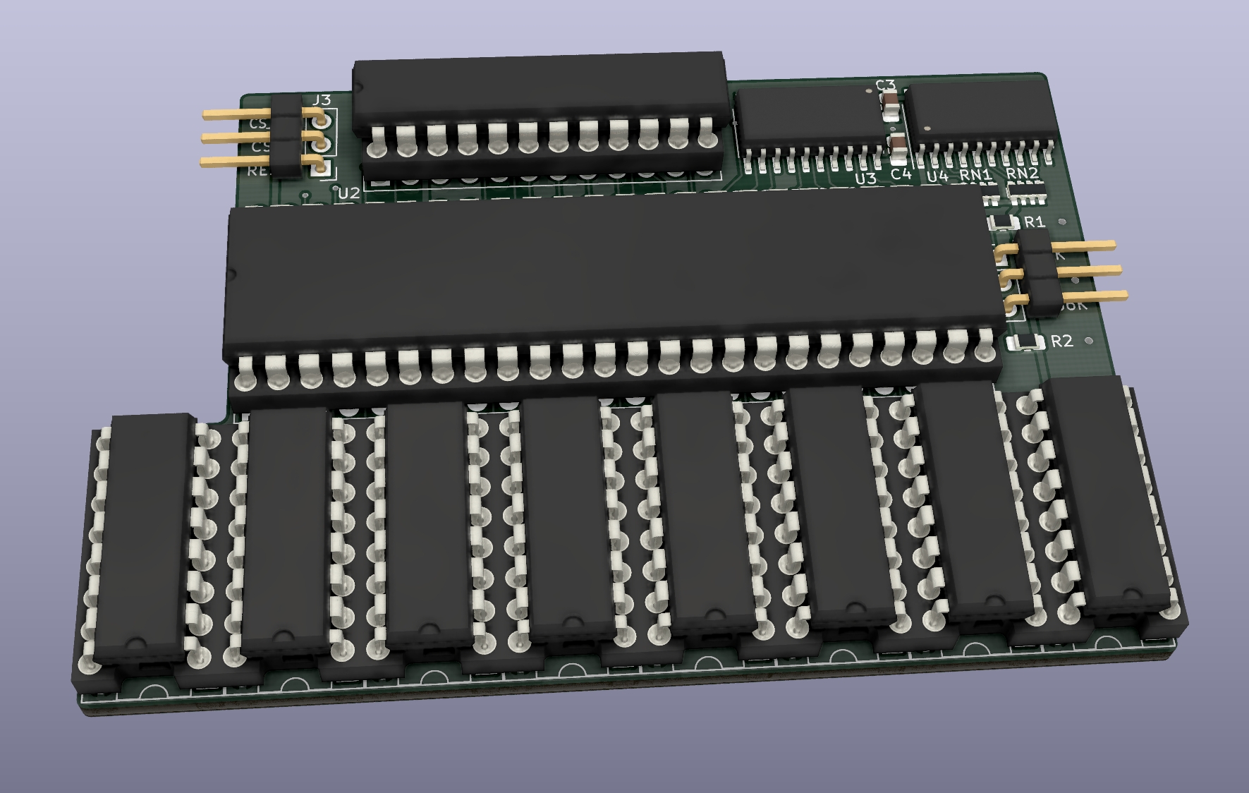
This project uses some SMD components due to space constraints, you are recommended to solder those first.
U5 and U6 can either be 74x157 or 74x257, as they are permanently enabled. I recommend using chips from the HCT family, but LS will do. Do NOT use HC.
Be careful with U3 and U4: these chips come in different widths. The board is made for 5.30 mm wide chips (which are the ones indicated in the BOM), you can probably fit wider ones but you are on your own.
The actual 41256 RAM chips have been out of production for ages but they can still be bought on AliExpress & similar sites.
You can connect a switch to U2 if you want to be able to switch back to 16 kB without having to open the case again. Honestly I just wouldn't bother, there is virtually no software that requires no more than 16 kB and it should just be fixed if this is really the case.
The board was accurately sized to fit alongside the CPU in a C16, but if you are using a CPU replacement it might just not physically fit. The same applies if you are using a Commodore 116, on which the board is not tested but it should theoretically work. I am sorry for that, feel free to redesign it and adjust the shape accordingly, it's easy to do with open source hardware.
Finally, U2 can either be a GAL20 or a GAL22: the former you can buy cheaply from AliExpress while the latter can be found new made by Atmel (ATF22-whatever). Whichever you choose, make sure to program it with the corresponding file from the gal directory.
I have used NEC D41256C-15 chips for my own testing. These have 150 ns access time which is probably as slow as you can go (The TED architecture should work even with 200 ns but I doubt you will find any RAMs that are that slow). This probably means that many other - if not all - 256k x 1 RAMs will work.
The board needs 3 wires from J3 to be connected to some points on the C16 mainboard. You can either solder them or use clips and perform a fully solderless installation.
On the C16:
CS_OUTmust be connected to pin 10 of U11.CS_INmust be connected to the LIFTED pin 16 of U16: remove the chip from the socket and carefully bend pin 16 so that it no longer gets inserted into the socket, then reinsert the chip and connect the clip to the now-dangling pin.RESETmust be connected to pin 2 of U9 or to pin 40 of U2, whichever is easier for you.
(See here for an explanatory picture.)
On the Plus/4 chip numbering is different, but if you're smart enough to fit the board, I'm sure you can also figure out the correct pins :).
No idea about the C116, sorry.
The basic idea behind the Hannes-style memory expansion mechanism is to intercept the Userport /CS range ($FD10-FD1F, PLA pin 16) and further decode it, feeding $FD10 only to its original purpose and using the remaining addresses for other stuff. In particular, $FD16 (64790) will be the control register for our RAM expansion (see ioarea.txt for further address assignments).
We are bound to using 41256 (256k x 1) RAM chips, as their internal matrix is organized in 256 rows by 1024 columns and thus only need rows A0-A7 for RAS-only refresh (which is the way the TED performs DRAM refresh). 44256 chips (256k x 4) would make life easier but they are generally organized in 512 rows and would need a much more complex refresh logic, in order to refresh the pages that are currently not selected.
This board has 14 chips (!) thus it is quite likely to significantly increase the power draw of your machine. Make sure to be using a good power supply.
Start with siz's memory test program: it must detect the 256 kB and the full test should complete without reporting any errors.
Then you can pick something from the Plus/4 World's 256k Support section: Future World and Dream World are perfect, and Taurin can be also a good candidate. Be aware that these old demos might use specific loaders that are unlikely to cooperate with an SD2IEC.
Note that some software from that section requires a different expansion (i.e.: Csory or something else): that will not work with Hannes256.
The expansion is controlled through a single 8-bit register at $FD16, whose individual bits control the memory configuration:
- Bit 0/1: Select RAM bank (0-3)
- Bit 2/3: Leave at 1 in order to allow compaibility with larger memory expansions
- Bit 4/5: Leave at 1 for compatibility with the expansion by CSORY
- Bit 6: "TED-feature" (added in "Update 1" of the original design):
- 0: TED always accesses the default bank (see below)
- 1: TED accesses the RAM-bank selected with bits 0 and 1
- Bit 7: Set the switch bound:
- 0: >= $1000
- 1: >= $4000
It should now be apparent that Hannes-style memory expansions work by allowing switching among different 64 kB banks. A 256 kB expansion thus allows for 4 banks, but only 240kB can actually be used, since memory lower than $1000 cannot be switched. A further restriction is possible through bit 7.
There is a concept of default bank (also called standard bank), which is the bank that:
- is automatically selected at power-up
- is accessed by the TED when bit 6 of the control register is cleared
- is accessed for all addresses < $1000 (or < $4000 when bit 7 of the control register is set)
This bank is indicated as bank 3 in Solder's notes, but this might be misleading: keep in mind that bits 2 and 3 of the control register must always be set to 1, so it's better the think of it as bank 15. With a 256 kB expansion this is the same bank as bank 3 but with larger expansions this would not be the case, so if you want maximum compatibility for your software, remember to always keep bits 2 and 3 at 1.
If you want to get this board produced, you are recommended to get the latest release rather than the current git version, as the latter might be under development and is not guaranteed to be working.
Every release is accompanied by its Bill Of Materials (BOM) file and any relevant notes about it, which you are recommended to read carefully.
The Hannes256 documentation, including the design itself, is copyright © SukkoPera 2022-2023 and is licensed under the Creative Commons Attribution-NonCommercial-ShareAlike 4.0 International License.
This documentation is distributed as is and WITHOUT ANY EXPRESS OR IMPLIED WARRANTIES whatsoever with respect to its functionality, operability or use, including, without limitation, any implied warranties OF MERCHANTABILITY, SATISFACTORY QUALITY, FITNESS FOR A PARTICULAR PURPOSE or infringement. We expressly disclaim any liability whatsoever for any direct, indirect, consequential, incidental or special damages, including, without limitation, lost revenues, lost profits, losses resulting from business interruption or loss of data, regardless of the form of action or legal theory under which the liability may be asserted, even if advised of the possibility or likelihood of such damages.
If you want to get some boards manufactured, you can get them from PCBWay through this link:

You get my gratitude and cheap, professionally-made and good quality PCBs, I get some credit that will help with this and other projects. You won't even have to worry about the various PCB options, it's all pre-configured for you!
Also, if you still have to register, you can use this link to get some bonus initial credit (and yield me some more).
You can also buy me a coffee if you want:
- Hannes and Solder for the original design and documentation.
- Levente Hársfalvi (TLC) for plenty of help, in particular with the MOS 6529 replacement circuit.
- siz for the memory test utility.