Chapter 3: NOT Gate. Inv
Examples of this chapter in github
Let's model our first combinatorial circuit: an inverter (NOT Gate).
Combinatorial circuits operate on the input bits, and then output the result. They don't store bits, they just modify them. The simplest of them all is the NOT gate, which has an input bit and an output bit. The output is always the inverse of the input. "0" turns into "1", and "1" turns into "0".
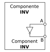
We'll name our component INV. The input will be A, and the output will be B.
Description is similar to the "hello world" component "setbit.v", but now we have an input, and an output.:
    //-- inv.v
    //-- Component has an input (A) and an output (B)
    module inv(input A, output B);

    //-- Both the input and the output are "wires"
    wire A;
    wire B;

      //-- Assign the inverse of the input, to the output
      assign B = ~A;

    endmodule
We assign the negated input A, to the output B. We use the **~ operator** in front of the A to invert the signal (this is the same operator as in the C programming language).
Because it is a combinatorial circuit, and does NOT store information, A and B are defined as wires: information goes through them, but it's not stored.
We'll connect the output of the gate to the D1 LED on the iCEstick (pin 99). The input will go to the 44 pin which can be reached through the expansion port of the iCEstick.
We want to enter a "0" or a "1" to the 44 pin from outside, in order to turn on or off the LED. To achieve this we will physically wire that pin to the Vcc pin (3.3v) or to ground (0v, GND).
Synthesis is done like always, with the make sint command:
$ make sint
This gates takes this resources:
| Resource | Usage |
|---|---|
| PIOs | 2 / 96 |
| PLBs | 1 / 160 |
| BRAMs | 0 / 16 |
This command uploads the resulting file into the FPGA:
$ sudo iceprog inv.bin
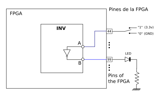
The iCEstick board has an expansion port connected to some of the pins of the FPGA. It's useful to solder a female pin strip to have easy access to them. You can see the strip soldered to the lower pins in the picture below.
The lower left pin is the 44 pin of the FPGA, and it's the one we´ll use as an input of the inverter. The lower right pins are 3.3v and GND, the first will be used to enter a "1", and the latter will be used to enter a "0".
Let's connect two pieces of cable, one into the 3.3v pin and the other to the GND pin.
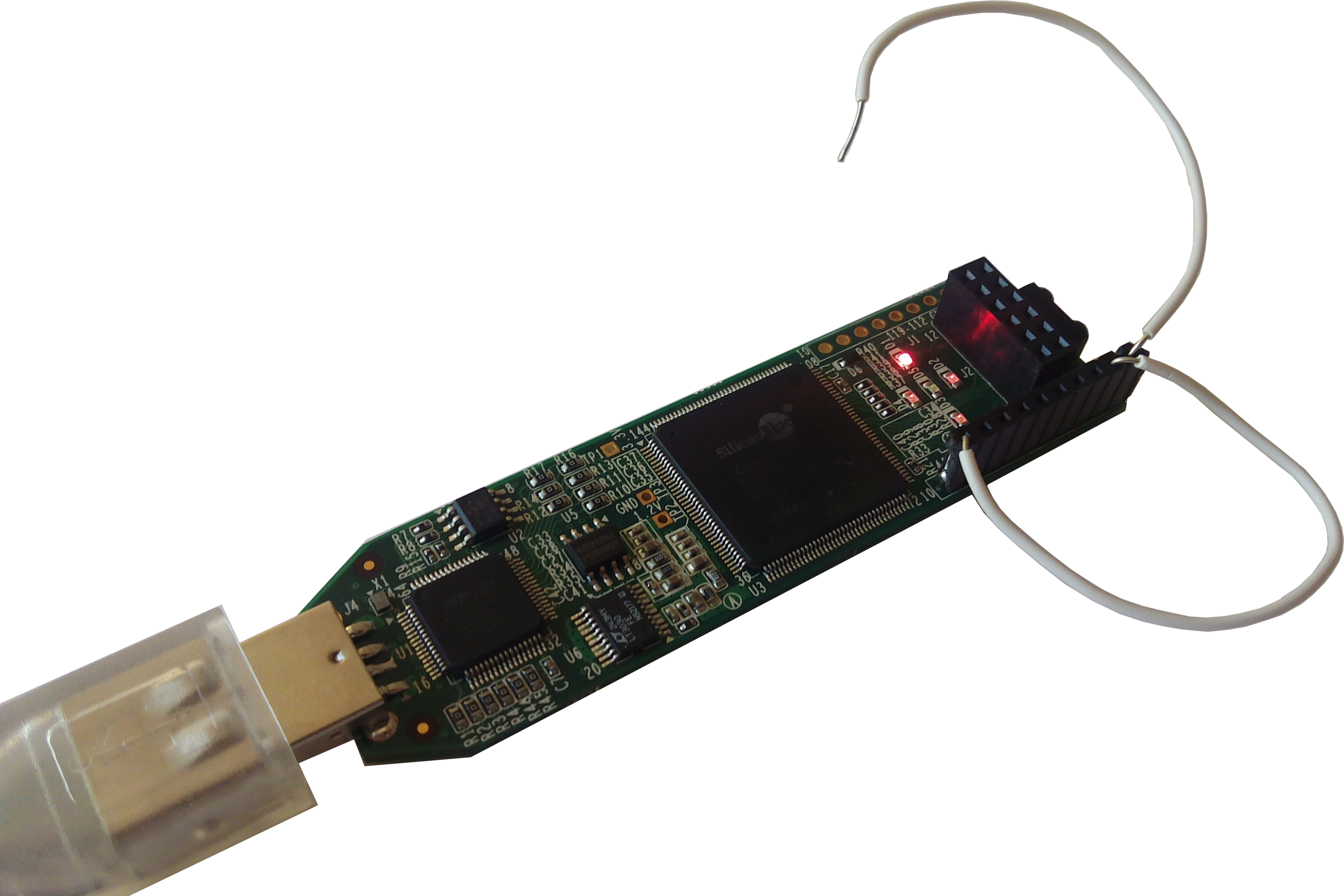
When the cable in the GND pin is connected to the 44 pin, the LED will turn on. When we connect the cable in the 3.3v, the LED turns off. When there is NOTHING connected to the 44 pin, the result is quite random: It can be on, it can be off, or it can be flickering between the two states. This is one of the basic rules of digital design: "Never leave an input wire unconnected. Always 1 or 0".
In the testbench, we must instantiate the inverter, and connect the dout wire to the B output.
We'll input various values, and check what comes out from the output. To do so, we connect the register named din.
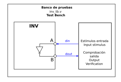
Unlike cables, registers work as a variable, to which we can assign different values. First we'll enter a "0", and then check that the output is a "1" (the negative). Then we do the other case: we enter a "1" and the check if we get a "0".
In the testbench, we instantiate the inverter, connecting it's input A to the register din, and it's input B to the dout cable. From the main loop, we assign values to din, and check dout.
    //-- inv_tb.v
    module inv_tb();

    //-- 1-bit register connected to the inverter's input
    reg din;

    //-- Wire connected to the inverter's output
    wire dout;

    //-- Instantiate the inverter, connecting din to the input A, and dout to the output B
    inv NOT1 (
     .A (din),
     .B (dout)
    );

    //-- Begin test
    initial begin

      //-- File to store the results
      $dumpfile("inv_tb.vcd");
      $dumpvars(0, inv_tb);

      //-- We put the input of the inverter to 0
      #5 din = 0;

      //-- After 5 time units, we check the output.
      # 5 if (dout != 1)
            $display("---->¡ERROR! Esperado: 1. Leido: %d", dout);

      //-- After another 5 time units, we change the input
      # 5 din = 1;

      //-- After 5 time units more, we check whether there is a 0 coming out the output
      # 5 if (dout != 0)
            $display("---> ¡ERROR! Esperado: 0. Leido: %d", dout);

      # 5 $display("FIN de la simulacion");
      # 10 $finish;
    end
    endmodule
We run the simulation by executing the make sim command:
$ make sim
In the simulation we can see that dout is always the inverse of din.
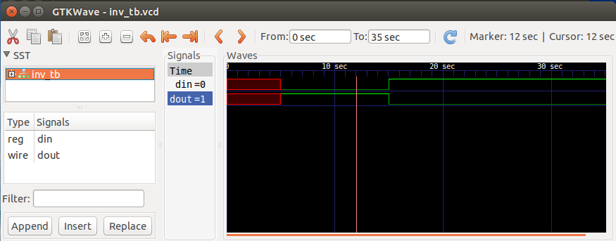
We can see that, in the first 5 time units, din and dout have the X value (red). This means that its value is undefined. That happens because we didn't initialize din with any value until the 5th time unit. Before that, it had an undetermined value (X) and therefore the output is undetermined too. After the 5th time unit, din is 0, and hence dout is 1.
- Make a component that has 2 inverters, and consequently, 2 inputs, and 2 outputs. Their outputs must be connected to 2 different LEDs.