Home
Documentation for the project will be located here as it is written. Updates are available at the bottom of this page.
The first version of the Serial Monitor is done and working. It has been a great way of finding out what things to improve for the next revisions and what's already working as it should.
Software for version 2 is written as fast as humanly possible and is documented here on the wiki.
More info on the mockup below can be found on the mockup page.
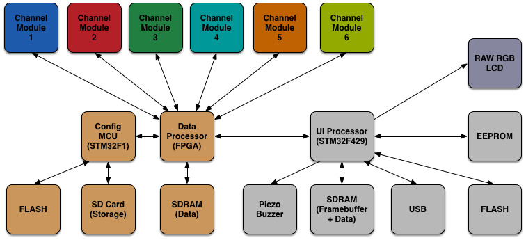
Mockup of version 2
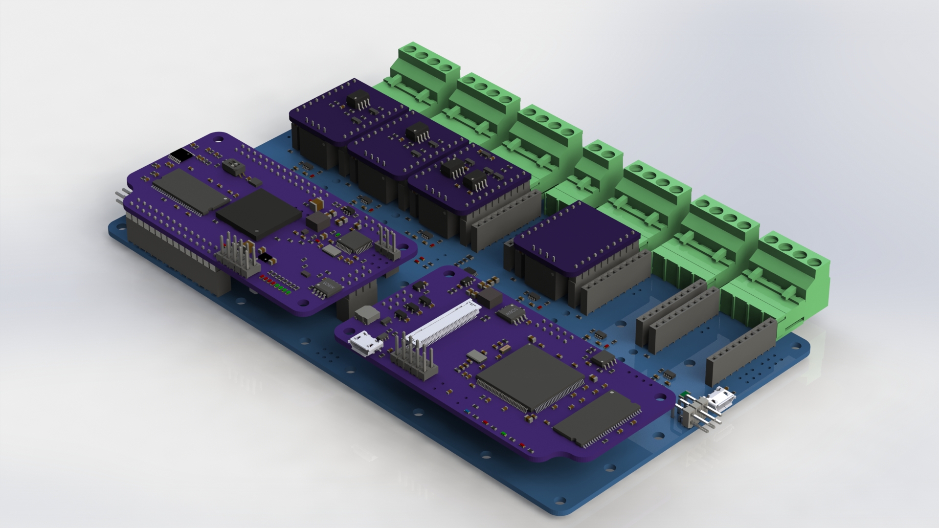
3D Rendering of the hardware
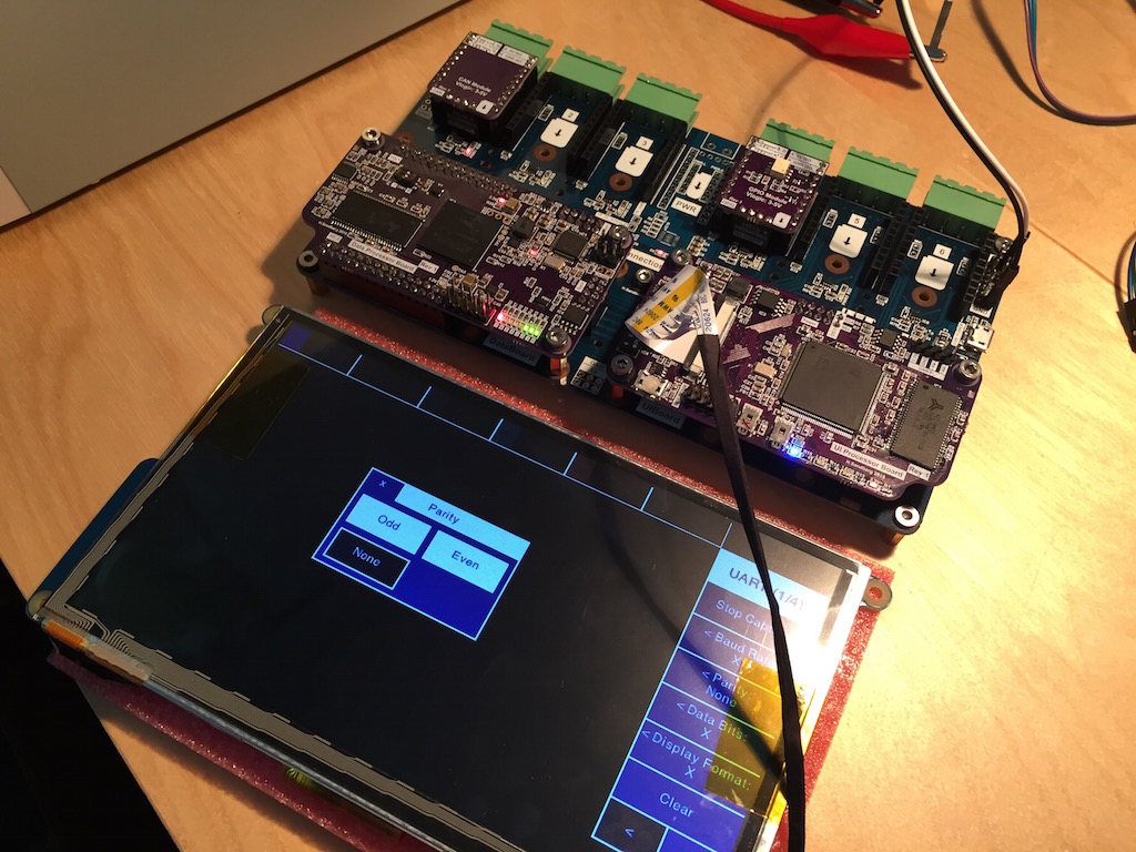
Under Development
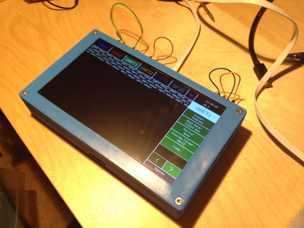
The serial monitor in its case
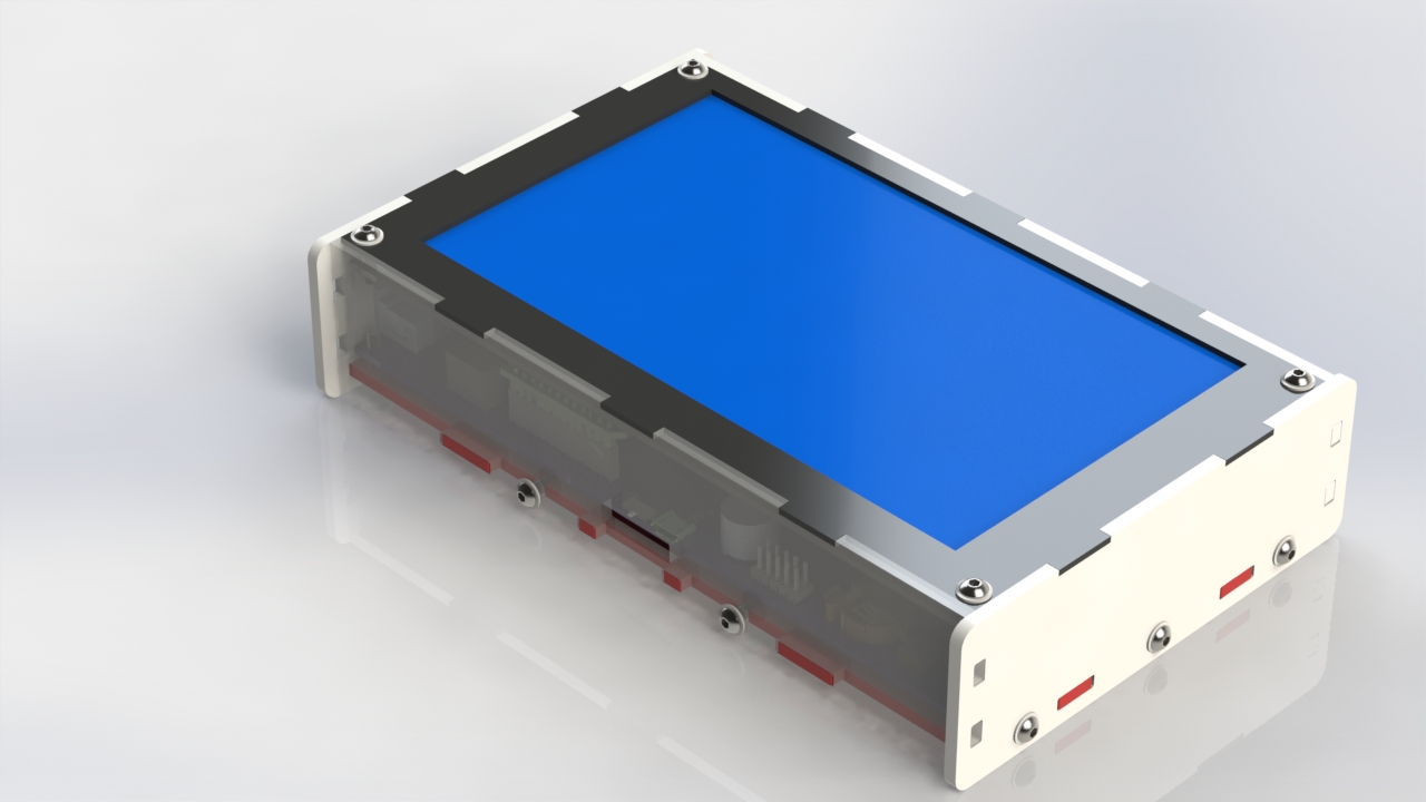
Rendering of a new case design made from laser cut acrylic
More pictures can be found here
This project is aiming to create a serial monitor for displaying data from various serial ports. The idea came from my recent purchase of a Rigol DG1032Z, which is an Arbitrary Waveform Function Generator. I started thinking what other types of equipment I could need in my electronics lab to help me with my projects. One thing that came to mind was this serial monitor, which you can connect to for example the TX and RX pins of an Arduino and display the data coming out there. The alternative would be to open up the Arduino Enviroment and the serial monitor there and therefore require a computer.
Inspiration was also taken from the oscilloscope I have, a Rigol DS1052E. It might seem like I'm trying to advertise for Rigol here but it's more like I'm on a student budget, though they are both great equipments I'm really happy with. Anyway, I wanted the GUI of the Serial Monitor to resemble that of an oscilloscope with different colors for the channels and a big section for the data you want to see. The mockup I've come up with is available on the GUI Mockup page of the wiki.
The first revision of the Serial Monitor has been a success and clearly demonstrated both positive and negative parts of the design that will be addressed in revision 2 which is currently worked on.
2015-11-28: Added more functionality to the fpga-config-over-uart software. As can be seen in the memory map for the fpga-config-mcu the bit file header now contains more information than just the size of the file. The added information is filename, modification date and a MD5 checksum.
2015-11-01: Upgraded to Quartus II 15.0.2. Did not seem to be that much different, some speed improvements were mentioned. One nice thing I've noticed is that in the RTL Viewer the registers are now grouped together more logically. If you have an 8-bit register it will display it as a stack of register instead of spreading each bit out over the screen. It makes it look better and more similar to what I draw by hand.
2015-10-24: After much hassle I've finally have an SPI slave running on the FPGA that is reliable. The problem I was having was that at random times the data read back from the FPGA would seem corrupt and would therefore mess up everything else. One big mistake was that I tried to implement the SPI slave so that it would process a byte and then immediately afterwards send the correct byte back. This proved to be too hard as we're only talking about half a SPI clock cycle to process the data and then make a decision about it. Therefore I relaxed the requirement and now the FPGA has eight SPI clock cycles to process the data and come up with a response.
2015-09-10: A lot of work has been done on getting the FPGA configuration working. A python script (fpga-config-over-uart) makes it possible to send bit files over uart to the config MCU on the data processor board. This MCU writes the bit file to the correct place in the SPI Flash and can then transfer it to the FPGA at startup whenever a command to do it is received.
2015-09-03: I have had some struggles with the touch controller for a couple of days now. More information about it can be found on the Touch Controller page. Some measurements I did on the FT5206 can be found here
2015-08-25: Note for future reference. The SDRAM controller on STM32F429 has two banks called 1 and 2. The different pins for these are called SDCKE0/SDCKE1 and SDNE0/SDNE1. Note that bank 1 maps to pins marked with 0 and bank 2 maps to pins marked with 1.
2015-08-15: As I will be writing most of the new software from scratch I've decided to update my software development tools. I'm using Eclipse together with GNU ARM Eclipse, great pieces of software that I highly recommend for anyone interested in developing for STM32.
2015-08-12: I have started to assemble some of the boards and discovered some errors in the connection board which meant I had to get some new ones made that I'm waiting for. The FPGA on the data processor board was a BGA device which is always scary to solder but after testing it seems like it was a success, all pins are connected where they should be. Now the focus will be on FPGA development and when the new connection board arrives everything can be put together.
2015-06-25: Made some small changes to the UI, see the GUI Mockup page.
2015-06-01: Ordered some PCBs for GPIO Module, CAN Module and RS-232 Module from OSH Park today. This is the first time I've ordered 4-layer board from them so it will be interesting to see how they compare to the 2-layer boards.
2015-05-29: Finished the design of the Connection Board. While doing this I discovered I had forgot to break out six signals from the Data Processor Board that will control the load switch for each module. As the connectors on the data board are already 2x15 pins it was hard to add them there. In the end I placed an I2C bus on the two unused pins on the power header instead which is then connected to a PCF8574 I/O expander on the connection board. As the power signals won't be used very often this seems like a reasonable compromise.
2015-05-25: Learned today that the LVDS interface on the Cyclone IV E FPGA need a VCCIO of 2.5V. I had connected all VCCIO pins to 3.3V for simplicity but this will not work as table 6-3 on page 6-12 in the handbook says it should be 2.5V. The LVDS signals I'm using are on bank 1 and 2 and I also have two LEDs on bank 1. My options are therefore to set VCCIO1 and VCCIO2 to 2.5V and use the LVDS interface or use external LVDS receivers and drivers as I'm using on the UI Processor Board. More information on how I solved this can be found on the FPGA LVDS page.
2015-05-14: The Data Processor Board is as good as finished. I still have to finish the HDL design to make sure it works with the pinout I use on the board. I probably have to wait until the boards are ordered and assembled before I can verify that the programming of the FPGA works as expected using the STM32F1 processor on board. The code for the SD-card interface can be developed before using the STM32F429 Discovery Board I have available. At the moment the plan is to have all the hardware assembled and ready for testing and integration by the end of the summer.
2015-05-04: Finally have a working SDRAM controller implemented on the FPGA. At this moment it is as simple as it can be but it is fully functional which is the important thing, later on when I have time I can optimize it. More information about the controller will be updated on the FPGA SDRAM page.
2015-04-17: Finished the design of the UI Processor Board. More work has been done on the GUI which has resulted in some new objects that should hopefully separate the graphical management from the data management, a bit MVC inspired I guess you could say. I've also been working on completing the LCD board that will connect to either a 50-pin LCD or a 40-pin LCD, there are some small differences between them that has to managed on the LCD board. Shouldn't take too long to finish it. Things that are left to do is Data Processor Board, Connector Board, RS-232 Module Board and FPGA design + integration with the MCU.
2015-03-17: FPGA design is still progressing nicely. Started work on some GUI changes to hopefully make it easier for the user but also to simplify the code needed to implement it. Some mockup images can be found here
2015-02-26: Been working on the FPGA design and finally found a bug I couldn't quite understand why I was getting but it makes sense now that I found the problem. Will continue on the FPGA design and hopefully I will get a hang of the working flow using Quartus II.
2015-01-17: Still working on the new version. I think I've decided on the new name: HexMon - Serial Monitor. "Hex" for six channels and "Mon" for monitor. Feels like it should be easier to say than just "Serial Monitor" as it was before. The new modular design feels good and I'm done with the CAN, GPIO and isolated power modules. The GPIO module is also used for UART or anything 5V/3.3V at reasonable data rate. The real benefit of the modular design will be that it's possible to configure the HexMon however one might want. Maybe someone wants to have six CAN channels or any other combination which will be possible now. It also brings down the price a bit as you don't have to populate all six channels. Right now the biggest cost comes from the isolation implemented on all modules and that is something I want, but as other people have other needs it is possible to design a non-isolated module as well which will definitely bring the cost down!
2014-11-28: One of the biggest reasons I started this project was because I had entered in a competition held by Prevas called Prevas Student Embedded Awards. After many hours of designing and coding I presented my project to them and after a couple of days I got the great news that I had won! This means a lot to have the support and appreciation from a company like Prevas and to know they believe in my idea. For this I'm very thankful and it will help a lot now that I'm moving forward with the next revision of the project. A press release in Swedish can be found here
2014-11-14: Made some changes to the wiki to make it easier to get around and also to prepare for the revision 2 content that is coming.
2014-11-07: Finally found a big bug in the code that caused the whole program to hang because something was corrupting the RAM and registers. It turned out to be bad coding on my side as I didn't do any sanity check on a subtraction which led to overflow and then everything turned bad fast. More info can be found in commit 3932ef6.
2014-10-22: Started work on what needs to be done for the next revision of the Serial Monitor. More information can be found on the Revision-2-Mockup page.
2014-10-15: Today I received a new LCD I ordered from Haoyu Electronics. More info can be found on the new LCD HY070CTP-HD page.
2014-10-11: Decided a few days ago to start reworking how data is read from memory and displayed in a GUITextBox. Took a few versions before I settled on the one in commit 31f5d5e. Now each GUITextBox is basically responsible of reading data from SPI flash and keeping track of the start and end address of the displayed data. Hopefully this will make it easier to continue with the development. I've already notice a speed improvement in the scroll as it's using the DMA better now!
2014-10-08: After finally getting the hang of the advanced timers I have now implemented frequency control of the PWM on the GPIO channel. I also added the buzzer for when a button is pressed but this can be turned off under the settings tab.
2014-10-07: Note on using STM32F4 TIM1 and TIM8 which are so called "advanced timers". I had connected the GPIO1 pin to TIM8_CH3N but for some reason I couldn't get it to work. The problem was the "N" in the name which implies it's the complementary output so I needed to set that one up which used another function call in the HAL library. The changes can be seen in commit cbd79ce
2014-10-06: I have now printed a first version of the case that actually fits and works. Some small adjustments can be done but this will work for now. An image of the case can be seen here
2014-09-16: More hardware bugs found, but fortunately this one was an easy fix. On the CAN transceiver I chose (TJA1050T/3) there's a pin called V_IO that I didn't connect because on other transceivers like the SN65HVD1050 that I looked on first, this pin is called Vref which is an output voltage reference that is Vcc/2. But the V_IO pin on the TJA1051T/3 is an input that determines the voltage of the IO pins so it should be connected to Vcc.
2014-09-14: A lot of work has been done on the UART channels and the GUI so that scroll now is functional and data can be written and read from the SPI FLASH. Next thing to do are the CAN channels.
2014-09-12: BIG FAT NOTE regarding the STM32CubeF4! If you want to have a UART remember to use the UART library files NOT the USART library files. I learned this the hard way!
2014-09-09: I received the PCBs on september 5th and assembled one immediately. For some reason it wouldn't work when I tried to program it and when I followed to code execution during a debug session there was an indication that something was wrong with the external oscillator. One look at the schematic and the problem was obvious, the two oscillators are connected to the opposite pins! It was therefore trying to run the MCU on 32.768 kHz instead of 8 MHz. Unfortunately the fix required me to cut some traces on the board and solder some jumper wires but now it works at least.
2014-08-17: The PCB is now done and ordered from OSH Park. It should arrive in the beginning of september.
2014-06-01: The LCD is now working using a STM32F4DISCOVERY board. More test are to be done but now we know the pin connections are correct.